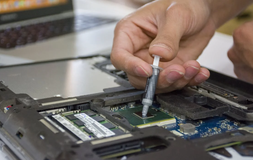
Thermal pads usually fail because the interface loses full, stable contact. The pad itself may be damaged, but that is only one possibility. Wrong thickness, poor compression, unsuitable hardness, uneven clamping, bad placement, contamination, and long-term aging can all increase thermal resistance.
A higher W/mK rating cannot rescue an air gap. It also cannot fix a heat sink that has been lifted away from a neighboring chip by an overly thick pad.
So, the useful question is not simply, “Is this a bad thermal pad?” It is:
What changed in the complete path from the heat source, through the pad, and into the cooling structure?
That path includes the component, pad, heat sink, housing, fasteners, tolerances, operating environment, and assembly process. Troubleshooting works best when all of them are checked together.
What Does Thermal Pad Failure Actually Mean?
A thermal pad is a preformed thermal interface material. It fills space between a heat-producing component and a cooler surface, such as a heat sink, cold plate, metal housing, shield, or chassis.
The pad replaces trapped air with a material that transfers heat more effectively. It may also provide electrical insulation, cushioning, vibration control, or production-friendly placement. HAKTAK’s broader thermal interface material guide explains how pads fit beside grease, putty, gels, phase-change materials, graphite, and conductive adhesives.
Failure means the interface no longer performs one or more required functions. It does not always mean the pad has cracked or melted.
Thermal Failure
Thermal failure can appear as:
- Higher junction, case, memory, or hot-spot temperature
- Thermal throttling
- Lower power output
- Fans running faster than before
- Unexpected shutdowns
- A large temperature difference between similar units
- One local hot spot while the average temperature looks acceptable
Mechanical Failure
Mechanical failure may include:
- Pad extrusion from the interface
- Tearing, puncture, or edge damage
- Permanent deformation
- Loss of recovery after long-term compression
- Movement under vibration
- PCB bending
- Component or solder-joint stress
- Heat sink or housing distortion
Electrical and Production Failure
Many pads perform more than a thermal job. A pad can transfer heat while still failing the assembly in another way.
Possible examples include:
- Reduced dielectric margin after over-compression
- Puncture over a sharp component edge
- Conductive graphite exposed near a circuit
- Contamination of contacts, optics, or conformal coating
- Adhesive transfer from the release liner
- A pad shifted away from its target area
- A protective liner left in place
- Placement variation that causes production scrap
That is why “the temperature looks fine” is not a complete acceptance test.
Bad Thermal Pad Symptoms and What They Usually Mean
The table below is a starting point, not a final diagnosis. Several failure causes can create the same symptom.
| Observed Symptom | Likely Cause Group | First Check |
| Temperature rises immediately after pad replacement | Wrong thickness, hardness, position, or liner handling | Pad imprint and full stack height |
| VRAM gets cooler but GPU core gets hotter | Pads lift the cold plate away from the GPU die | Core paste imprint and pad compression |
| One side of a module is hot | Tilted heat sink, housing warp, uneven torque, or partial coverage | Flatness, fastening sequence, and contact pattern |
| Temperatures vary widely between production units | Tolerance, placement, torque, or material-lot variation | Gap distribution and process records |
| Performance drifts after months | Compression set, material aging, chemical exposure, or fastener relaxation | Aged thickness, recovery, and thermal impedance |
| Pad squeezes out around the edges | Excess thickness, pressure, softness, or missing mechanical stops | Compression at the minimum gap |
| Pad looks oily | Formulation bleed, heat aging, or environmental interaction | Supplier limits and nearby contamination |
| Intermittent electrical fault appears | Puncture, compressed insulation, contamination, or conductive edge exposure | Dielectric path and final compressed thickness |
| Pad sticks to the liner or stretches during removal | Liner aging, adhesive transfer, or material too soft for the process | Release force and handling method |
The timing of the symptom is useful. A problem that begins immediately after assembly usually points toward geometry, compression, placement, or fastening. A slow drift is more likely to involve aging, compression set, vibration, chemical exposure, or movement in the stack.
Why the Wrong Thermal Pad Thickness Causes Overheating
Wrong thickness is one of the most common thermal pad failure causes. It also creates some of the most confusing symptoms.
The nominal CAD gap is not enough. Real products have variation from component height, solder thickness, PCB warpage, housing flatness, heat sink machining, gasket compression, and screw torque.
A pad must work at the minimum, nominal, and maximum gap.
What Happens When a Thermal Pad Is Too Thin?
A pad that is too thin may not touch both surfaces. Even if it makes light contact at nominal conditions, it can lose contact at the largest gap.
The result may include:
- Air pockets
- Weak contact marks
- High interface resistance
- Local hot spots
- Temperature variation between units
- Intermittent contact during vibration
This failure can be hard to see through the side of an assembly. A pad may appear to sit in the correct location while carrying almost no pressure.
What Happens When a Thermal Pad Is Too Thick?
A thicker pad is not automatically safer. It creates a longer heat path and often requires more force to reach the installed thickness.
An overly thick pad can:
- Increase bulk thermal resistance
- Bend a PCB
- Stress solder joints or packages
- Deform a thin housing
- Extrude around the edges
- Reduce electrical insulation margin after severe compression
- Prevent another component from touching the same cold plate
This last point is easy to miss.
Suppose a GPU cooler contacts the GPU die, memory chips, and power components. New memory pads are thicker or harder than the original parts. They make strong contact with the memory, but they hold the cold plate slightly above the GPU die. Memory temperature may improve while GPU core and hot-spot temperatures become much worse.
The memory pad looks like it is working. The complete cooling assembly is not.
For a practical selection method based on the full gap range, see HAKTAK’s guide to selecting thermal pad thickness for electronics.
A Simple Thickness Example
Assume a 1.5 mm pad is installed across a gap that varies from 1.0 mm to 1.35 mm.
| Gap Condition | Installed Gap | Pad Compression | Possible Result |
| Minimum gap | 1.00 mm | 33% | Force may be high for a firm pad |
| Nominal gap | 1.20 mm | 20% | May be suitable if supplier data supports it |
| Maximum gap | 1.35 mm | 10% | Contact may be weak for some materials |
The same pad can be close to over-compressed in one unit and under-compressed in another. That is why one nominal percentage is not enough.
Under-Compression and Over-Compression Failure
Thermal pads need pressure to conform to surface texture and replace trapped air. More pressure is not always better, though. There is a useful operating window.
Under-Compression Leaves Hidden Air Gaps
Under-compression can happen when:
- The pad is too thin.
- The pad is too hard for the available load.
- Screw torque is too low.
- The housing flexes instead of loading the pad.
- The surfaces are tilted.
- The pad area is large relative to the total clamp force.
- Component heights vary more than expected.
Large pad area deserves attention. Pressure equals force divided by area. A pad that becomes twice as large needs twice the force to reach the same average pressure, assuming other conditions remain equal.
The interface may look neatly covered but still have poor surface wetting.
Over-Compression Creates Mechanical and Electrical Risk
Over-compression can temporarily improve contact. The thermal gain may become very small after full contact is reached, while mechanical risk keeps rising.
Possible results include:
- Pad extrusion
- Permanent compression set
- PCB bow
- Package cracking
- Solder-joint strain
- Fastener overload
- Housing distortion
- Puncture over sharp edges
- Reduced final dielectric thickness
A soft pad may tolerate high strain with modest force. A firm pad at the same strain may load the assembly much more heavily. Compression percentage cannot be reviewed without the force-deflection curve.
Calculate the Compression Window
The basic compression equation is:
Compression (%) = (supplied thickness – installed thickness) / supplied thickness x 100
Run this calculation at:
- Minimum gap
- Nominal gap
- Maximum gap
Then compare every condition with supplier compression data and the assembly’s force limit. HAKTAK’s detailed guide to thermal pad compression ratio covers this process and the related dielectric concerns.
Pad Hardness and Conformability Can Break a Good Design

Thermal conductivity often gets the large print on a datasheet. Hardness and compression force may get a small graph near the back. In real products, that small graph can decide whether the thermal path works.
Why a High-Performance Pad May Be Too Hard
Highly filled materials can be firmer. That is not automatically bad. A firm pad can offer dimensional stability and easier handling.
Trouble starts when the product cannot provide enough pressure to compress it.
The pad may:
- Touch only surface peaks
- Fail to follow enclosure curvature
- Overload fragile components
- Hold a heat sink above another device
- Produce different results as screw torque varies
Shore hardness is useful for screening, but it does not fully describe assembly behavior. Two pads with similar Shore 00 values can have different stress-versus-strain curves.
Ultra-Soft Pads Have Their Own Problems
Very soft pads conform well at low pressure. They are useful over delicate components and wide height variation.
Still, soft material can be awkward. It may:
- Stretch during liner removal
- Tear around narrow features
- Move during assembly
- Extrude under high compression
- Stick to tools or gloves
- Lose dimensional accuracy in unsupported shapes
The best choice is not “soft” or “hard” by itself. It is the material that reaches full contact inside the allowed force window and remains stable through production and service.
Poor Contact, Surface Flatness, and Assembly Tolerance
A thermal pad can only conform so far. It cannot repair unlimited housing warp, a tilted heat sink, or a badly located fastener.
Rough, Warped, and Tilted Surfaces
Common causes of uneven contact include:
- Heat sink machining tolerance
- Cast housing distortion
- PCB warpage
- Component height differences
- Solder thickness variation
- Uneven gasket compression
- Thermal expansion mismatch
- A screw boss that acts as an early mechanical stop
If one side of a pad compresses by 30% and the other side barely touches, temperature will not be uniform.
Contact paper, pressure-sensitive film, temporary witness material, 3D measurement, cross-sectioning, or a controlled pad-imprint inspection can help reveal the pattern. Each method has limits, so it should be used carefully.
Uneven Screw Torque Can Tilt the Interface
Fastening one corner completely before the others can tilt the heat sink. It is a bit like tightening one leg of a wobbly table and hoping the other three follow.
A controlled sequence may include:
- Bringing all screws into light contact
- Tightening in a cross pattern
- Applying torque in two or more stages
- Using calibrated tools
- Recording final torque
- Adding mechanical stops where required
Torque is only an indirect measure of clamp force. Friction, thread condition, washer design, and housing stiffness also matter.
Pad Footprint and Misalignment
An undersized pad can leave part of the heat source uncovered. An oversized pad may add force over areas that do not transfer useful heat.
Poor geometry can also create:
- Interference with screw bosses
- Folded edges
- Material over connectors or test points
- Narrow sections that tear during liner removal
- Electrical-clearance problems
- Placement ambiguity for operators
Good die-cut design should follow the useful thermal overlap while allowing realistic placement tolerance.
And yes, check the liners. A clear PET liner can be surprisingly hard to notice. Leaving it in place adds a poorly controlled insulating layer and blocks the pad from conforming.
Why High W/mK Thermal Pads Can Still Fail

Thermal conductivity describes a bulk material property. It does not directly report the temperature of a GPU, MOSFET, battery module, LED, or controller.
The complete interface includes:
- Bulk resistance through the pad
- Contact resistance at both surfaces
- Final compressed thickness
- Effective contact area
- Heat spreading in the component and housing
- Airflow, liquid cooling, or natural convection after the heat leaves the interface
Thickness Can Outweigh a Conductivity Advantage
Ignoring contact resistance for a simple comparison: R = t / (k x A)
For the same contact area:
- A 10 W/mK pad at 2.0 mm gives a simplified t/k value of 0.20.
- A 5 W/mK pad at 0.8 mm gives a simplified t/k value of 0.16.
In this example, the lower-conductivity pad has lower bulk resistance because it is much thinner. Real interfaces also contain contact resistance, so this is not a product ranking. It is a reminder to check the whole geometry.
Compare Thermal Impedance at Realistic Pressure
Thermal impedance data can be more useful than W/mK when the test thickness, pressure, temperature, and surface conditions are known. HAKTAK’s article on thermal conductivity versus thermal impedance explains why those conditions must travel with the reported value.
A pad tested at high laboratory pressure may look excellent. The same material can perform poorly in a lightweight plastic enclosure with low clamp force.
This is also why high W/mK does not always mean better cooling performance. The label matters, but the installed interface matters more.
Thermal Pad Aging, Compression Set, and Loss of Contact
Some failures are present on the first day. Others develop slowly.
A pad can pass initial thermal testing and still lose contact after heat aging, thermal cycling, vibration, chemical exposure, or years under compression.
Compression Set
Compression set is the permanent deformation left after a material has been compressed for a defined time and then released.
In an assembly, high compression set can contribute to:
- Lower recovery
- Reduced contact pressure
- Greater sensitivity to tolerance or housing movement
- Higher thermal resistance
- Poor rework behavior
- Local hot spots after aging
The problem is not always visible. The pad may remain in place but no longer push firmly against both surfaces.
Fastener relaxation and gasket aging can make this worse. Several parts in the stack may lose load at the same time.
Hardening, Softening, and Chemical Change
Long exposure to heat can change polymer behavior. The direction and amount depend on the formulation.
A pad may:
- Become harder
- Become softer
- Lose elasticity
- Change surface tack
- Show increased oil bleed
- Swell after fluid exposure
- Lose adhesion to a carrier or reinforcement
Materials near oil, fuel, coolant, cleaning agents, plasticizers, or process chemicals need compatibility testing with the actual fluid. A generic label such as “chemical resistant” is too broad for reliable design.
Thermal Cycling and Power Cycling
Semiconductor packages, copper, aluminum, PCB laminates, solder, and polymers expand at different rates. Every heating and cooling cycle moves the stack a little.
Repeated movement can:
- Change pressure distribution
- Rub or shear the pad
- Increase edge damage
- Relax fasteners
- Open a small contact area
- Shift a poorly retained pad
- Stress adhesive or reinforcement layers
Solid pads are generally less prone to classic grease pump-out. They can still lose effective contact through mechanical movement and compression set.
Vibration and Shock
Automotive electronics, industrial equipment, rail systems, outdoor telecom hardware, and mobile devices experience vibration or impact.
Vibration can reveal:
- Inadequate pad retention
- Abrasion against sharp edges
- Fastener relaxation
- Housing movement
- Weak adhesive
- A design with almost no compression margin
The temperature may remain stable during a short bench test and drift only after environmental exposure.
Oil Bleed, Contamination, Delamination, and Adhesive Failure
Not every thermal pad failure is a simple thickness problem.
Is Oil Bleed Always a Failure?
Some silicone-based pads can show a small amount of surface oil or low-molecular-weight material. The acceptable amount depends on the formulation and application.
Minor bleed does not automatically prove poor heat transfer. However, migration can become a serious concern near:
- Electrical contacts
- Relays
- Optical assemblies
- Cameras and sensors
- Conformal coatings
- Paint or bonding surfaces
Acceptance should follow supplier limits and application testing, not a quick visual opinion.
Dust, Fingerprints, and Cleaning Residue
Soft, tacky surfaces attract contamination. Dust and fibers can create local contact defects. Oil from handling can interfere with adhesion. Aggressive cleaning residue may change the surface or attack nearby materials.
Good handling controls may include:
- Keeping liners in place until assembly
- Holding pads by liner tabs or edges
- Using clean gloves or tools
- Protecting cut parts in sealed packaging
- Controlling cleaning chemistry
- Separating silicone-free materials from silicone-contaminated tools where necessary
Pressure-Sensitive Adhesive Can Add Another Failure Layer
Adhesive backing helps placement, but it also adds thickness and another interface.
Possible problems include:
- Adhesive transfer to the liner
- Uneven tack
- Air trapped during placement
- Edge lifting
- Poor adhesion after heat or humidity
- Residue during rework
- Higher thermal resistance
Full-area adhesive should not be added by habit. Natural tack, selective adhesive, split liners, or mechanical retention may work better in some designs.
Reinforcement and Laminate Delamination
Pads may contain fiberglass, PET, PEN, graphite, or other carrier layers. Reinforcement improves handling and puncture resistance, but a layered construction introduces more interfaces.
After heat, humidity, chemical exposure, or repeated flexing, inspect for:
- Separation between layers
- Bubbles
- Cracked edges
- Wrinkles
- Carrier exposure
- Loss of electrical isolation
Thermal Pad Failure Modes Change by Material
The phrase “thermal pad” covers several material families. Their risks are not identical.
| Material Family | Typical Strength | Likely Failure Concerns | Useful Mitigation |
| Silicone gap pad | Soft gap filling, cushioning, and insulation | Compression set, bleed, tearing, siloxane sensitivity | Match hardness, pressure, and aged requirements |
| Silicone-free pad | Suitable near sensitive contacts, optics, or coatings | Different stiffness, adhesive aging, moisture response | Validate contamination and mechanical behavior |
| Fluorosilicone pad | Better resistance to many oils and fuels | Higher cost and fluid-specific compatibility | Test actual fluid, temperature, and duration |
| Graphite sheet or pad | Thin in-plane heat spreading | Creasing, tearing, edge conductivity, poor large-gap filling | Protect edges and add insulation where needed |
| Phase-change pad | Thin interface with improved hot-state wetting | Activation mismatch, coating movement, poor cold contact | Test start-up, cycling, and operating temperature |
| Thermal putty | Covers uneven component heights | Application-volume variation, residue, and movement | Control mass, placement, and final gap |
| Liquid gap filler | Fills complex geometry at low assembly stress | Dispense voids, mixing, cure, rework, and chemistry-specific movement | Monitor dispensing and cure process |
For conventional compressible sheet interfaces, HAKTAK’s silicone thermal pad range provides options around thickness, hardness, tack, dielectric performance, and custom die-cut formats.
When component heights vary too much for one sheet thickness, thermal putty versus thermal pad selection becomes relevant. A dispensable thermal conductive gap filler may also reduce assembly stress in complex or large-area interfaces.
The alternative still needs validation. Changing material families replaces one set of risks with another; it does not remove engineering work.
Thermal Pad Failures by Application and Industry
The same basic physics applies across industries, but the most important failure mode changes with the product.
GPUs, AI Servers, and High-Power Accelerators
These assemblies may use pads on memory, power stages, controllers, and heat spreaders. Several components often share one cold plate.
Key risks include:
- Wrong replacement thickness
- Hard pads lifting the cold plate from a GPU or accelerator package
- Incomplete VRAM coverage
- Uneven screw torque
- Service technicians mixing several thicknesses
- High local heat flux hiding behind an acceptable average temperature
Monitor core, hot-spot, memory, inlet, and coolant temperatures where available. One sensor cannot tell the whole story.
MOSFETs, IGBTs, and Power Modules
Power electronics often need heat transfer and electrical insulation at the same interface.
Watch for:
- Puncture over package edges
- Reduced dielectric thickness after compression
- High clamp force
- Heat sink flatness
- Power-cycling movement
- Local pressure around screws
Electrical testing should be repeated after mechanical and environmental stress, not only on fresh material.
EV Batteries and BMS Electronics
Battery systems may have large interfaces, multiple height levels, flexible trays, and strict stress limits.
Common failure paths include:
- Large total compression force
- Cell or PCB loading
- Coolant exposure
- Gap variation across a wide area
- Vibration
- Assembly movement over long service life
A material selected from one small test coupon may behave differently over a large battery module.
Automotive ECUs and ADAS Modules
Automotive housings face temperature cycling, vibration, humidity, oils, cleaners, and long qualification periods.
Traceability matters here. A production failure may come from a material lot, a housing change, screw-torque drift, or a new liner process. Root-cause analysis should preserve all four possibilities.
LED Modules
LED reliability is strongly linked to temperature. Pads or insulating sheets may sit under metal-core boards, drivers, or housings.
Uneven board contact can create local hot spots even when case temperature looks reasonable. Optical contamination and long heat exposure can also influence material choice.
Telecom, Industrial, and Outdoor Electronics
These products may run continuously in sealed or partly sealed enclosures.
Relevant concerns include:
- Humidity
- Dust
- Continuous high temperature
- Enclosure distortion
- Long service intervals
- Limited maintenance access
A low-cost pad replacement can become an expensive field visit. Long-term validation matters more than saving a few minutes in the lab.
How to Find the Root Cause of a Thermal Pad Failure
Replacing the pad immediately may hide the evidence. A controlled workflow is more useful.
Step 1: Confirm the Thermal Symptom
Compare the unit under consistent conditions:
- Ambient and inlet temperature
- Power or workload
- Fan or pump speed
- Firmware and control settings
- Heat sink cleanliness
- Sensor location
- Test duration
A dirty heat sink or changed fan curve can look like a pad failure.
Step 2: Map the Cooling Path
Write down the path:
Component -> thermal pad -> spreader or housing -> heat sink -> air or coolant
Mark every contact and every possible bottleneck. The pad may not be the dominant resistance.
Step 3: Inspect Contact Evidence
Before cleaning the assembly, photograph:
- Pad position
- Compression marks
- Core paste imprint
- Torn or folded edges
- Oil or residue
- Liner condition
- Screw locations
- Areas with no visible contact
Poor paste imprint on a neighboring die is strong evidence that pad thickness or stiffness has changed the stack.
Step 4: Measure the Real Stack-Up
Measure or calculate:
- Minimum, nominal, and maximum gap
- Supplied pad thickness
- Compressed thickness
- Component height
- Housing and heat sink flatness
- PCB bow
Avoid measuring a soft used pad with uncontrolled finger pressure. That number can be nicely precise and still wrong.
Step 5: Review Force and Fastening
Check:
- Screw torque
- Tightening sequence
- Clip or spring load
- Thread condition
- Mechanical stops
- Gasket interaction
- Total pad area
A torque change can affect both thermal contact and board stress.
Step 6: Separate Cause Categories
| Cause Group | Examples |
| Material | Wrong grade, hardness drift, contamination, aging, damaged liner |
| Design | Wrong gap, weak clamp layout, poor flatness, low dielectric margin |
| Process | Misplacement, liner left on, mixed thickness, torque variation |
| Environment | Heat, vibration, humidity, oil, coolant, cleaning chemicals |
This separation prevents every problem from becoming a supplier complaint before the assembly has been checked.
Step 7: Change One Variable at a Time
Do not change the pad brand, thickness, paste, screw torque, fan curve, and heat sink at the same time. The new temperature may improve, but the reason will remain unknown.
Use controlled A/B samples where possible.
Step 8: Verify the Fix After Stress
A corrective action should survive:
- Heat aging
- Temperature cycling
- Power cycling
- Vibration
- Humidity or fluid exposure where relevant
- Reassembly or service handling
Initial temperature is necessary. It is not lifetime evidence.
Thermal Pad Testing Standards and Reliability Checks
No single test certifies the complete thermal pad interface.
ASTM D5470 for Thermal Impedance
ASTM D5470-17(2024) covers steady-state thermal impedance measurement and calculation of apparent thermal conductivity for thermally conductive electrical insulation materials.
It is useful, but the standard itself notes that idealized test conditions do not directly match most applications. Pressure, thickness, temperature, specimen area, and surface conditions should be reported with the result.
Hardness and Compression Set
ASTM D2240 is commonly used for durometer hardness. ASTM D395 addresses compression set for rubber materials.
These properties support material comparison, but they do not replace a full force-deflection curve or assembled validation. A small coupon in a laboratory does not know that a real PCB is thin, warped, and loaded by four screws.
Environmental Testing
IEC 60068 methods are often used to structure temperature change, vibration, shock, damp heat, and related environmental tests.
The exact profile should match the product. Five mild cycles do not prove suitability for an automotive module expected to survive years of repeated thermal and mechanical stress.
Flammability and Dielectric Requirements
UL 94 classifications describe material flammability behavior under defined tests. They do not prove low thermal impedance, compression stability, or electrical insulation in a compressed and aged assembly.
Dielectric testing should consider:
- Final compressed thickness
- Edge geometry
- Puncture risk
- Humidity and contamination
- Thermal aging
- Mechanical cycling
Test the Complete Assembly
Official AMD guidance for thermal interface materials emphasizes spreading, mounting pressure, and elimination of air gaps. Those factors explain why material data must be connected to the actual cooling assembly.
Reliability should also measure thermal performance after exposure, not merely confirm that the pad remains visible. A Parker Chomerics gap-pad reliability report illustrates this approach by tracking thermal impedance through thermal shock, thermal cycling, and vibration stages.
For a broader map of test methods, HAKTAK’s guide to common TIM testing standards explains why the method and test conditions must be reported beside the value.
Common Thermal Pad Failure Causes and Solutions
| Failure Cause | Typical Evidence | Corrective Action |
| Pad too thin | Little or no imprint at the maximum gap | Increase thickness or use a more conformable gap-filling material |
| Pad too thick | High force, extrusion, or lost contact elsewhere | Reduce thickness and recalculate the compression window |
| Pad too hard | Weak surface contact under available load | Choose lower modulus or revise the clamp design |
| Excessive compression | Board bow, pad squeeze-out, or reduced insulation margin | Add mechanical stops, reduce thickness, or lower force |
| Uneven torque | One-sided imprint or corner hot spot | Define torque, tools, and tightening sequence |
| Poor flatness | Uneven compression across the pad | Improve housing, heat sink, or support design |
| Misplacement | Part of the heat source remains uncovered | Add alignment features, tabs, or vision inspection |
| Compression set | Temperature rises after service time | Qualify aged recovery and select a more stable grade |
| Chemical incompatibility | Swelling, softening, hardening, or residue | Test actual fluids and change material chemistry |
| Contamination | Poor contact, adhesion loss, or electrical concern | Improve packaging, cleaning, and handling controls |
| Adhesive or liner problem | Stretching, residue, bubbles, or edge lift | Change liner, tack level, adhesive pattern, or assembly method |
| Wrong TIM family | One pad cannot follow the gap or movement | Evaluate putty, gel, PCM, graphite, or liquid gap filler |
When to Replace the Pad and When to Redesign the Interface
Replace the pad when it is:
- Torn
- Folded
- Punctured
- Contaminated
- Permanently deformed
- Missing identification
- The wrong grade or thickness
- Removed from an assembly without an approved reuse process
Redesign the interface when:
- No single pad thickness covers the full tolerance range.
- Required compression overloads the PCB or component.
- The heat sink remains tilted or warped.
- A pad is being used to compensate for a structural problem.
- Field failures return after repeated pad replacement.
- The interface needs both very low stress and large gap coverage.
Repeatedly changing pads in a bad mechanical stack is like putting new tires on a bent wheel. The new part may help for a while, but the underlying geometry is still waiting.
Conclusion
Thermal pads rarely fail because of one number on a datasheet. They fail as part of an interface system.
Wrong thickness can leave an air gap or lift a shared heat sink away from another chip. Poor compression can reduce contact. Excessive compression can damage the pad, PCB, component, or dielectric path. Aging, vibration, chemicals, contamination, adhesives, and assembly variation can then change a design that looked fine on day one.
The practical solution is to diagnose the entire heat path. Measure the real gap. Check minimum, nominal, and maximum compression. Review hardness and force. Inspect contact evidence. Control placement and torque. Then test thermal, mechanical, and electrical performance after realistic environmental stress.
The best thermal pad is not simply the one with the highest W/mK. It is the one that keeps reliable contact without overloading the product through its intended life.
Frequently Asked Questions
What Are the Signs of a Bad Thermal Pad?
Common signs include rising component temperature, thermal throttling, high fan speed, inconsistent temperatures between units, poor contact marks, cracking, tearing, hardening, extrusion, oil migration, or loss of elasticity. These symptoms can also come from incorrect thickness, poor fastening, dust, airflow, or heat sink problems, so the complete cooling system should be checked.
Can Thermal Pads Cause Overheating?
Yes. A pad can cause overheating when it is too thin to make contact, too thick to fit the stack, too hard to compress, badly positioned, contaminated, or installed with a liner still attached. Thick or firm pads can also lift a shared cold plate away from a CPU or GPU die.
What Happens If a Thermal Pad Is Too Thick?
An overly thick pad can increase thermal resistance and assembly force. It may bend the PCB, stress components, squeeze out around the edges, reduce dielectric thickness, or prevent a neighboring component from touching the heat sink. The result can be worse temperatures even when the new pad has a higher conductivity rating.
What Happens If a Thermal Pad Is Too Thin?
A pad that is too thin may not contact both surfaces, especially at the maximum production gap. This leaves insulating air pockets and creates hot spots. Contact can also become intermittent during vibration or thermal cycling.
How Much Should a Thermal Pad Compress?
There is no universal compression percentage for every pad. The correct value depends on thickness, hardness, force-deflection behavior, surface flatness, pad area, gap tolerance, and component stress limits. Compression should be calculated at minimum, nominal, and maximum gap and compared with supplier data.
Do Thermal Pads Lose Effectiveness Over Time?
They can. Heat, compression set, thermal cycling, vibration, humidity, chemical exposure, and fastener relaxation may reduce contact or change material behavior. A pad can remain visually intact while its installed thermal impedance increases.
Is Oil Coming from a Thermal Pad a Sign of Failure?
Not always. A small amount of bleed can be formulation-dependent. Excessive migration may still contaminate contacts, optics, coatings, or bonding surfaces. Acceptance should follow supplier limits and thermal, electrical, and contamination testing for the application.
Can Two Thermal Pads Be Stacked?
Stacking creates an extra interface where air, misalignment, and contact resistance can develop. It also makes compression less predictable. A single correctly selected pad is normally preferred. Stacking should only be used when the supplier and product validation support it.
Can a Removed Thermal Pad Be Reused?
Reuse is generally risky. A removed pad may be torn, contaminated, stretched, or permanently compressed. Its final thickness and pressure may no longer be repeatable. Production, high-power, and reliability-critical equipment should normally receive a new specified pad.
Why Did GPU Temperatures Rise After Replacing Thermal Pads?
The replacement pads may have the wrong thickness, hardness, or position. They may be holding the cooler away from the GPU die, or they may not contact the memory and power components. Check the GPU paste imprint, pad compression marks, screw sequence, all liners, and the exact original thickness requirements before trying another material.