
Thermal Pads for Electronics, EV Batteries and Power Devices
Haktak supplies thermal pads that fill gaps, improve surface contact, provide electrical insulation and transfer heat from components to heat sinks, housings, cold plates or metal frames.
Thermal Pad Selection Inputs
Start with real assembly geometry before choosing W/mK or hardness.
What Are Thermal Pads?
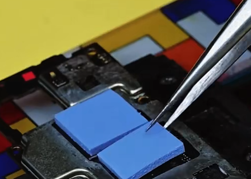
Thermal pads are soft, pre-formed thermal interface materials used between heat-generating components and cooling surfaces. They fill air gaps, conform to surface roughness, support electrical insulation and help transfer heat through a controlled bond line thickness.
Where Thermal Pads Are Used
Thermal pads are commonly used when assemblies need clean placement, controlled thickness, electrical insulation and tolerance compensation.
EV Battery Systems
Used around battery modules, BMS areas, control units, charging electronics and power conversion components.
Power Electronics
Support thermal contact for MOSFETs, IGBTs, power supplies, inverters, drivers and metal housings.
LED Lighting
Transfer heat from LED boards, modules or drivers to housings and heat spreaders.
Telecom and Data Equipment
Fit compact, high-density assemblies where chips or modules need repeatable heat dissipation.
Industrial Electronics
Protect stable thermal performance in controls, sensors, drives, power modules and outdoor devices.
Consumer Electronics
Provide gap filling and heat transfer in compact designs where clean assembly is important.
Thermal Pad Material Options
Thermal pads can be tuned for conductivity, softness, compression, insulation and process needs. Haktak can support standard pads and custom pad structures for specific assembly requirements.
- Silicone thermal pads: flexible, conformable and widely used for electronics thermal management.
- Electrically insulating thermal pads: designed for heat transfer with dielectric protection.
- Soft gap pads: useful for fragile components, uneven surfaces and lower assembly pressure.
- Custom die-cut pads: supplied in shapes, thicknesses and formats matched to the assembly.
How to Choose Thermal Pad Thickness
Thermal pad thickness should be selected from the full mechanical tolerance stack, not only the nominal gap. A pad must contact both surfaces at the maximum gap while avoiding excessive compression at the minimum gap.
| Design Input | What to Check | Why It Matters |
|---|---|---|
| Minimum gap | Smallest possible gap after tolerances | Prevents over-compression, PCB bending, housing deformation or component stress. |
| Nominal gap | Expected assembly gap under normal production | Helps define target compression and thermal impedance. |
| Maximum gap | Largest possible gap after tolerances | Ensures the pad still contacts both surfaces without air gaps. |
| Surface flatness | Warpage, machining marks, molded part variation | Affects real contact area and local hot spots. |
| Available pressure | Screws, clips, housing preload or compression limit | Determines whether the pad can conform without excessive force. |
| Electrical clearance | Voltage level, dielectric strength, insulation distance | Prevents electrical failure in battery, LED and power applications. |
Compression, Hardness and Thermal Performance
Thermal pads need enough compression to improve contact, but too much compression can damage components or reduce reliability.
| Parameter | What It Means | Selection Guidance | Risk if Wrong |
|---|---|---|---|
| Compression ratio | Percentage reduction in pad thickness after assembly | Use supplier data and test min/nominal/max gap conditions. | Too low causes air gaps; too high may stress boards and components. |
| Hardness | Pad softness or resistance to compression | Softer pads fit fragile or uneven assemblies; harder pads may need more pressure. | Wrong hardness can cause poor contact or mechanical damage. |
| Thermal conductivity | Bulk material heat transfer rating | Compare with bond line thickness and real thermal impedance. | High W/mK may not help if contact is poor. |
| Compression set | Permanent thickness loss after long-term compression | Validate under temperature, pressure and aging conditions. | Can reduce contact pressure and increase thermal resistance over time. |
Thermal Pad vs Other Thermal Interface Materials
| Material | Best For | Advantages | Limitations to Check |
|---|---|---|---|
| Thermal pad | Controlled gaps, clean assembly, electrical insulation | Pre-formed, easy to place, die-cut, stable thickness | Needs compression and proper thickness selection |
| Thermal gel | Uneven gaps, automated dispensing, low stress | Good wetting, no die cutting, adaptable volume | Dispensing control and pumpability must be validated |
| Thermal grease | Thin bond line with clamping pressure | Low contact resistance and good wetting | No gap support, pump-out and dry-out risk |
| Thermal adhesive | Bonding plus heat transfer | Provides mechanical attachment and thermal path | Rework, cure, stress and bond line control |
| Thermal potting | Encapsulation and environmental protection | Protects electronics and helps spread heat | Repairability, exotherm, shrinkage and component stress |
Application Matrix
| Application | Typical Pad Direction | Key Requirements | Validation Focus |
|---|---|---|---|
| EV battery electronics | Electrically insulating soft thermal pad | Dielectric strength, low stress, aging resistance | High-voltage insulation, thermal cycling, compression set |
| Power modules and inverters | Higher-conductivity thermal gap pad | Thermal impedance, operating temperature, mechanical pressure | Device temperature, gap tolerance, dielectric margin |
| LED lighting | Insulating pad or die-cut thermal pad | Stable contact, heat aging, clean assembly | LED temperature, adhesion or placement stability, aging |
| Telecom and data equipment | Soft gap pad or custom die-cut pad | Repeatable thickness, low contact resistance, long-term compression | Thermal cycling, pressure retention, module temperature |
| Industrial electronics | Durable thermal interface pad | Vibration resistance, insulation, environmental aging | Field aging, humidity, dust, thermal shock |
Custom Thermal Pad Development
Haktak can support custom thermal pad solutions based on material properties, thickness, hardness, die-cut shape, insulation needs and production process.
Define the gap
Measure min, nominal and max gap with tolerance stack-up and surface flatness.
Match the pad
Select conductivity, thickness, hardness, dielectric performance and compression range.
Prototype and test
Validate thermal impedance, pressure, contact marks, insulation and mechanical reliability.
Prepare production
Optimize die cutting, release liner, packaging, handling and quality consistency.
Need Help Selecting a Thermal Pad?
Send your gap range, heat source, cooling surface, target temperature, voltage requirement, available pressure and assembly drawing. Haktak can recommend a standard thermal pad or develop a custom pad solution.
Related Technical Guides
What Is a Thermal Pad?
Learn how thermal pads work and where they fit in electronics thermal design.
Read guideThermal Pad Compression Ratio
Understand how much compression is enough and what happens when compression is too high or too low.
Read guideHow to Select Thermal Pad Thickness
Review the relationship between gap tolerance, compression and thermal performance.
Read guideThermal Pads FAQ
What is a thermal pad used for?
A thermal pad is used to fill the gap between a heat source and a cooling surface. It improves surface contact, reduces air gaps and helps transfer heat while often providing electrical insulation.
How do I choose thermal pad thickness?
Choose thickness based on the minimum, nominal and maximum gap after tolerance stack-up. The pad should contact both surfaces at the maximum gap without excessive compression at the minimum gap.
Is higher W/mK always better for thermal pads?
No. Higher thermal conductivity can help, but real performance also depends on bond line thickness, compression, contact area, hardness and thermal impedance in the final assembly.
Are thermal pads electrically insulating?
Many thermal pads are electrically insulating, but not all. Engineers should confirm dielectric strength, volume resistivity and voltage requirements before use.
Can thermal pads be customized?
Yes. Thermal pads can be customized by thickness, hardness, conductivity, die-cut shape, liner format, size, color and electrical insulation requirements.
When should I use thermal gel instead of a thermal pad?
Thermal gel can be better for complex or uneven gaps, automated dispensing and low-stress assemblies. Thermal pads are better when clean placement, controlled thickness and die-cut shapes are preferred.