
Heat transfer + EMI attenuation
Thermal Electro-Magnetic Absorber Pads for Heat Transfer and EMI Control
A thermal electro-magnetic absorber pad combines a compliant thermal path with electromagnetic-loss behavior in one compressed interface. It is considered when a hot RF or high-speed component sits close to a shield, housing or noise-sensitive circuit and a conventional gap pad cannot address both problems.

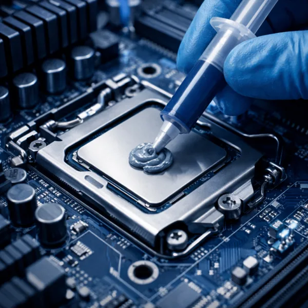
What Is a Thermal Electro-Magnetic Absorber Pad?
A thermal electro-magnetic absorber pad is a preformed, usually compliant interface material engineered to transfer heat while dissipating part of the incident electromagnetic energy inside the material. It can bridge a controlled gap between a component and a shield, housing, heat spreader or other cooling structure while adding frequency-dependent loss near an RF noise source.
The phrase describes a function, not one universal formulation. The matrix may be silicone or non-silicone, the filler system may include thermally conductive particles and magnetic or dielectric loss components, and the construction may be homogeneous or laminated. Thickness, compression and the surrounding metal geometry influence the result.
That is why the material should be evaluated within the broader thermal interface material selection framework. A pad that looks strong in a thermal conductivity table can still be ineffective at the failing frequency. An absorber with promising free-space data can still create a poor thermal contact or overload a shield cover.
Transfer heat
Replace insulating air and create contact from the hot component to a defined cooling boundary.
Absorb energy
Introduce electromagnetic loss in the location and frequency range where unwanted coupling occurs.
Fit the stack
Provide repeatable thickness, compression and die-cut geometry for production assembly.
How a Thermal EMI Absorber Pad Handles Two Energy Paths
Heat flow and electromagnetic coupling are different physical problems. They may share a location, but one data point cannot stand in for the other. Map each path before selecting the material.
For heat, the important boundaries include source temperature, contact area, surface roughness, compressed thickness, spreading structure and ambient or coolant condition. For EMI, the important boundaries include source, frequency, field location, coupling mechanism, sensitive receiver, nearby metal and absorber placement.

Move component heat into the cooling structure
The compressed pad replaces air, conforms to height variation and connects the hot component to a shield, cover or housing. The final result includes both contact boundaries and heat spreading beyond the pad.
Reduce unwanted coupling near the noise source
Loss mechanisms inside the pad dissipate part of the electromagnetic energy at the target frequency. Location, thickness, field orientation and nearby conductive geometry determine whether the system gains useful EMC margin.
Thermal EMI Absorber Pad vs Thermal Pad, EMI Sheet and Shielding Gasket
These materials can look similar after die cutting, but their primary functions and validation methods are different. Select by the failure mechanism and interface duty.
Thermal EMI absorber pad
Best when one compressed location must transfer heat and attenuate electromagnetic energy.
Validate thermal impedance, frequency response, compression, electrical behavior and system EMC together.Conventional thermal gap pad
Bridges a controlled gap and conducts heat to a spreader, enclosure or sink. It is not automatically an EMI absorber.
Compare familiar silicone thermal pad constructions when EMI loss is not required.Thin EMI absorber sheet
Targets noise suppression or reflection control where gap filling and substantial heat transfer may not be required.
Its thin film structure may fit antennas, flex cables and covers but may not replace a soft thermal interface.Conductive shielding gasket
Provides electrical contact between conductive structures for grounding and enclosure shielding.
It is not automatically a thermal interface or absorber. Ground path resistance and corrosion may dominate.Frequency Response and EMI Absorption Metrics
“Good EMI absorption” is not a complete specification. Absorber behavior changes with frequency, thickness, field orientation, backing metal, sample dimensions and test fixture. Ask for a curve or stated data at the band that matters.
The material may be described with attenuation, insertion loss, reflection loss, return loss, power loss, complex permeability or complex permittivity. These values are not interchangeable. Confirm what was measured and whether the fixture represents the final location.
Keep the thermal result equally grounded in conditions. The guide to thermal conductivity versus thermal impedance explains why bulk W/m·K cannot predict the final joint by itself.
Frequency range
Define the emission, resonance, susceptibility or coupling issue in MHz or GHz. Broadband language is not enough when one narrow peak causes the failure.
Attenuation or loss
Record the reported unit, test fixture, sample dimensions, thickness and backing condition. A dB value without context cannot be transferred safely.
Complex permeability
Magnetic-loss materials may be characterized by real and imaginary permeability. Their relevance depends on the frequency band and field coupling.
Complex permittivity
Dielectric properties influence impedance matching, electric-field loss and interaction with antennas or transmission structures.
Thickness and backing
Absorption may change when the material is compressed, placed against metal or moved relative to the noise source. Test the intended stack.
EMC margin
The decision metric is the final emission, immunity, signal integrity or receiver result with production-representative hardware.
Thermal EMI Absorber Pad Material Constructions
No single construction is best for every frequency, temperature, pressure or cleanliness requirement. Treat the matrix, filler system, carrier and surface layers as a complete material.
 01
01Silicone elastomer composite
Widely used for compliance, temperature stability and natural tack. Thermally conductive and absorber fillers are dispersed in a soft matrix.
Check siloxane, bleed, contamination and customer material restrictions where sensitive surfaces are nearby. 02
02Silicone-free elastomer
Used when silicone chemistry is restricted, while still providing a soft, preformed interface and absorber function.
Confirm the exact silicone-free definition, outgassing method, residue behavior and long-term compression. 03
03Homogeneous gap pad
A single compliant body can provide uniform handling and avoid a hard boundary between absorber and thermal layers.
Uniform appearance does not mean isotropic thermal or electromagnetic behavior; review test orientation. 04
04Composite or laminated pad
Separate functional layers can tune surface contact, absorber behavior, reinforcement or electrical isolation.
Layer interfaces add thickness and may affect thermal resistance, bending, die cutting and delamination risk.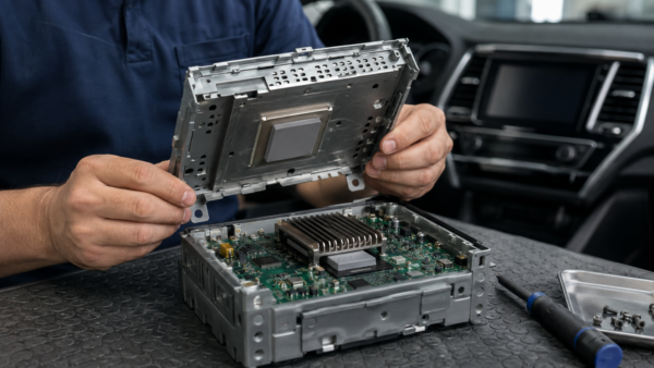 05
05Carrier-reinforced construction
A film, fabric or mesh may improve converting, dimensional stability and placement of thin or complex shapes.
The carrier can change compression, puncture behavior, dielectric performance and through-plane heat flow. 06
06Adhesive or natural-tack surface
Natural tack can simplify placement. A pressure-sensitive adhesive can control one-sided attachment or liner presentation.
Any adhesive layer becomes part of the thermal and RF stack; include it in qualification samples.Thermal Electro-Magnetic Absorber Pad Specifications That Matter
A useful data sheet connects every number to a method, specimen and condition. Request curves where the response changes with frequency or compression.

Conductivity and impedance
Record direction, method, specimen thickness, pressure and temperature. Prefer interface-relevant impedance or resistance data when available.
Frequency response
Request attenuation or absorption across the actual problem band, with sample thickness, backing and fixture clearly stated.
Thickness and tolerance
Specify incoming thickness, permitted tolerance and final compressed thickness across minimum, nominal and maximum gaps.
Hardness and stress
Use pressure–strain or stress–compression information for the delivered construction, not hardness alone.
Isolation or conductivity
Confirm dielectric strength, volume resistivity, surface resistance and whether the design expects isolation, grounding or shield contact.
Temperature and aging
Separate storage, recommended continuous use, excursions and qualification profile. Track compression and RF response after aging.
Outgassing and residue
Define the risk to optics, contacts, coatings or sealed volumes. Silicone-free and low-outgassing are different requirements.
Sheet, roll and die-cut form
Record liner, natural tack, adhesive, carrier, tabs, holes, edge clearance, packaging and shelf-life conditions.
Select Thickness and Compression from the Real Interface
The pad must contact both surfaces at the largest assembled gap without applying unsafe force at the smallest gap. Nominal CAD distance is not enough. Measure tolerance, shield deflection, fastener behavior and the height of the hottest and noisiest components.
Compression improves surface conformity and normally reduces the pad thickness, but it can also change filler spacing and electromagnetic response. A very soft pad may protect fragile parts yet take compression set. A harder material may preserve geometry but load a shield cover, BGA solder joints or thin PCB.
Review how compression changes thermal pad performance, then extend the validation to the target EMI band.
Capture minimum, nominal and maximum values at each functional contact region.
Include components, shields, solder joints, fasteners, clips and enclosure flatness.
Confirm whether absorption or attenuation changes at the intended thickness and backing.
Trend temperature, force, thickness and EMC behavior after cycling and dwell.
Where Thermal Electro-Magnetic Absorber Pads Are Used
The best candidates combine localized heat, limited space and a defined EMI issue near a shield, cover or housing. Each application still needs its own frequency and thermal evidence.
 01 / TELECOM
5G Radios and RF Modules
Power amplifiers, RF transceivers, baseband processors and shielded radio compartments may need simultaneous heat transfer and noise attenuation.
Review telecom and 5G materials 02 / OUTDOOR RF
Sealed Radio and Network Hardware
Outdoor units add temperature cycling, humidity, sealing, vibration and corrosion to an already sensitive RF interface.
Plan thermal pads for 5G base stations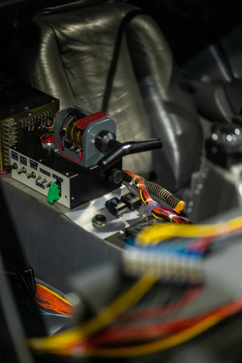 03 / AUTOMOTIVE
ADAS, Radar and Vehicle Electronics
Radar modules, ECUs and telematics hardware combine dense electronics, RF sensitivity, cycling, vibration and long qualification lives.
Explore automotive electronics materials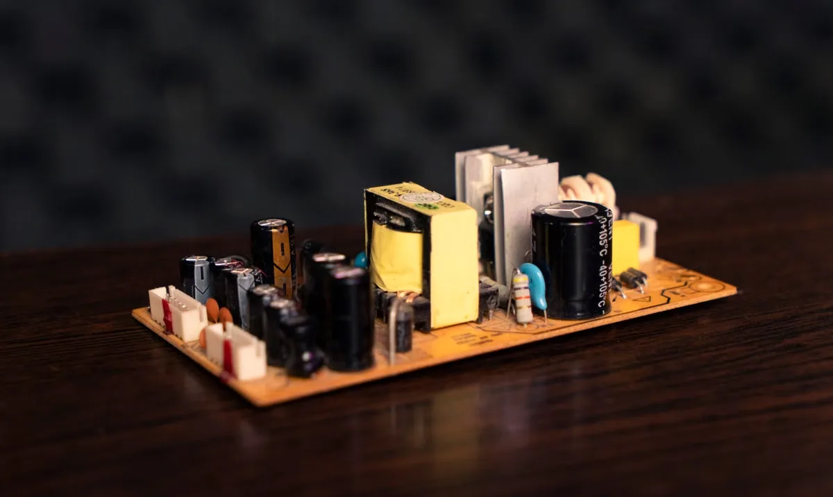 04 / POWER
Converters, Chargers and Drives
Fast switching edges and high dissipation can place thermal and electromagnetic problems close together around modules, magnetics and control circuitry.
See power electronics material options 05 / COMPUTE
Servers and High-Speed Digital Systems
Processors, memory, accelerators, optical links and high-speed I/O can produce both heat and noise inside restricted mechanical envelopes.
Review AI server and data center materials 06 / COMPACT
Displays, Cameras and Connected Devices
Small modules may position antennas, processors, displays and metal covers within millimeters of each other, leaving little room for separate materials.
View consumer electronics materialsHow to Select a Thermal Electro-Magnetic Absorber Pad
Send Your Thermal EMI RequirementsStart with the failed or at-risk system, not a catalog conductivity. Keep thermal, RF, mechanical, electrical and production constraints visible at the same time.
If the noise source is unknown, locate it first. If the thermal boundary is unknown, define it first. Screening material before those two steps produces an attractive data-sheet comparison but a weak engineering decision.
Can one material layer occupy both the correct thermal contact and the correct electromagnetic field location without violating pressure, electrical or production limits?
Map heat sources
Record normal and peak losses, temperature limits, contact areas, spreaders, shields, housings and ambient or coolant conditions.
Locate the EMI mechanism
Identify the noise source, failing frequency, coupling path, victim circuit, antenna or enclosure feature involved.
Measure the stack
Capture gap range, flatness, roughness, shield movement, fastener tolerance and available absorber volume.
Set electrical boundaries
Define isolation, grounding, shield continuity, voltage, creepage, edge clearance and allowed conductivity.
Screen constructions
Compare matrix chemistry, absorber evidence, thermal impedance, compression, carrier, tack and environmental data.
Prototype the final geometry
Use production-like die cuts, liners, holes, adhesive layers, pressure and metal backing before freezing the drawing.

Thermal, EMC and Reliability Validation Plan
Test the complete assembly with the intended shield, fasteners, board, cooling structure, pad geometry and software operating state. Coupon data narrows candidates; system data releases the design.
Haktak can support a structured screening plan through material selection and testing.
Incoming dimensions
Verify thickness, die-cut geometry, holes, liner, surface condition, mass where useful and material traceability.
Baseline thermal test
Measure temperature or resistance at recorded power, pressure, contact area, ambient and cooling conditions.
Baseline EMC test
Capture the failing emission, immunity, resonance, coupling or signal-integrity behavior before the candidate is installed.
Pressure sensitivity
Test minimum, nominal and maximum gap or load without overstressing the shield, board, package or solder joints.
Frequency sweep
Compare the relevant band, not one convenient point, and note whether the source or enclosure modes shift.
Thermal and power cycling
Trend temperature, thickness, compression and EMC margin through realistic operating cycles.
Environmental aging
Use the required heat, humidity, vibration, fluid, salt, vacuum or storage profile for the application.
Electrical safety
For insulating designs, verify dielectric strength, leakage, edge clearance and behavior after cutting and compression.
Post-test inspection
Check migration, cracks, delamination, residue, compression set, shield marks and loss of contact.
Pilot production run
Confirm placement, liner removal, orientation, inspection, rework, packaging and lot-to-lot repeatability.
Common Failure Modes for Thermal EMI Absorber Pads
Most failures are not caused by one weak catalog value. They occur when the material is tested or installed in a stack that differs from the design assumptions.
Strong data at the wrong frequency
The absorber curve looks impressive, but the failing emission or resonance lies outside the useful range.
Bulk W/m·K hides contact loss
Thickness, surface contact or the shield’s spreading resistance produces a higher component temperature than expected.
Material misses the field hot spot
The pad contacts the hot device but does not occupy the coupling region that controls the EMC result.
Shield and board are overloaded
Excess force bows the cover, stresses solder joints or changes contact and absorber behavior across the assembly.
Absorber is treated as a shield
A nonconductive absorber cannot automatically replace a grounded enclosure seam or conductive gasket.
Adhesive and carrier are ignored
Production samples add films or tack layers that change thickness, thermal resistance and electromagnetic response.
Compression set opens contact
Heat, cycling or vibration changes pressure distribution and reduces thermal or EMI performance over time.
Die-cut placement is not repeatable
Rotation, liner handling, holes, edge clearance and shield assembly move the pad away from the qualified geometry.

Prepare a Useful Brief for Custom Die-Cut Thermal EMI Absorber Pads
A complete brief helps separate a true dual-function need from a conventional thermal interface, thin absorber film or conductive shielding gasket. Estimated values are acceptable during early screening when assumptions are clearly identified.
Geometry belongs in the qualification plan. Holes, slots, edge clearance, tabs, adhesive zones and liner presentation can affect both placement and performance. Review the process for custom thermal pad die cutting before freezing production tooling.
Heat source, power, target temperature, cooling boundary, contact area and current material result.
Noise source, frequency band, test failure, coupling mechanism, target margin and absorber location.
Minimum, nominal and maximum gap, flatness, holes, shield features, keep-outs and tolerances.
Pressure window, fasteners, spring force, cover deflection, orientation, vibration and service access.
Isolation, voltage, grounding, shield contact, surface resistance and edge-clearance requirements.
Sheet, roll, die-cut or kiss-cut format, liner, adhesive, packaging, quantity and placement method.
Thermal Electro-Magnetic Absorber Pad FAQ
What is a thermal electro-magnetic absorber pad?
It is a preformed interface material designed to transfer heat and introduce electromagnetic loss in the same compressed location. It is used when one assembly region has both a thermal contact need and a defined EMI problem.
Is a thermal EMI absorber pad the same as a normal thermal pad?
No. A normal thermal pad primarily fills a gap and transfers heat. A thermal EMI absorber pad must also show useful, frequency-dependent absorber performance under relevant thickness and geometry conditions.
Does an absorber pad replace an EMI shielding gasket?
Not automatically. A shielding gasket normally creates conductive continuity and a ground path across a seam. An absorber pad dissipates electromagnetic energy. Some systems use both functions, but each must be validated separately.
Can thermal conductivity predict EMI absorption?
No. Thermal conductivity describes heat transport under a stated method. EMI absorption depends on complex material properties, frequency, thickness, field orientation, location and surrounding conductive geometry.
Which frequency range should be specified?
Specify the actual emission, resonance, susceptibility or signal-integrity problem range, plus the test method and desired margin. Do not request an undefined “broadband” material when one band controls the failure.
How does thickness affect performance?
Thickness affects thermal resistance, compression force, contact and electromagnetic response. Use the final compressed thickness and the intended metal backing or enclosure geometry when comparing candidates.
Are thermal EMI absorber pads electrically insulating?
Some are, but not all constructions should be assumed insulating. Confirm dielectric strength, volume and surface resistivity, cut-edge behavior and the final voltage or grounding requirement.
Are silicone-free thermal EMI absorber pads available?
Silicone-free constructions can be considered for sensitive optics, contacts, coatings or customer restrictions. The exact chemistry definition, outgassing, residue, thermal result and absorber evidence still require separate confirmation.
Can the material be custom die cut?
Yes. Depending on material and geometry, it can be supplied as sheets, rolls, individual parts or kiss-cut arrays with holes, slots, tabs, liners and selected adhesive zones.
What should be tested before production approval?
Measure baseline and aged thermal behavior, relevant EMC or RF performance, gap and pressure sensitivity, electrical safety, environmental durability, die-cut integrity, placement repeatability and pilot-line capability in the final stack.