
Thermal Pads for Electronics
電子機器向け熱伝導パッドとカスタム熱マネジメント
Bridge real gaps between heat-generating components and heat sinks, housings, spreaders or cold plates with a controlled, production-ready thermal interface. Compare material family, thickness, compression, insulation and custom format around the complete assembly—not one headline conductivity value.
議会内で
電子機器におけるサーマルパッドの仕組み
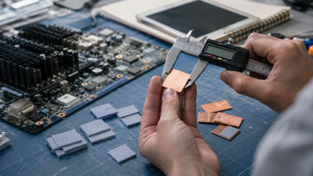
A thermal pad replaces thermally insulating air with a solid, conformable heat-transfer path. Its job is not simply to sit between two surfaces. It must remain in useful contact while the assembly moves through tolerance, fastening, temperature cycles and service life.

空隙と表面の凹凸を埋める
軟質パッドは、平面度誤差、部品高さのばらつき、表面テクスチャに沿って変形します。熱が界面を通過できる箇所を決めるのは、公称フットプリントだけではなく、実効接触面積です。.
Move Heat Into the Cooling Structure
The pad connects a device, package or board to a heat sink, metal housing, chassis or cold plate. Compressed thickness and interface resistance strongly influence the real temperature rise.

Preserve Electrical and Mechanical Separation
適切な熱伝導インターフェースパッドは、絶縁分離、緩衝、または制御されたスペーシングを実現できます。これらの機能は、打ち抜き加工、圧縮、環境曝露後に評価する必要があります。.
マテリアルファミリー
電子機器向けサーマルパッドの種類を比較
各製品群は、インターフェースに関する異なる課題を解決します。サンプルを依頼する前に、追従性、熱流方向、電気特性、汚染リスク、使用環境、生産形態を比較してください。.
 01
01シリコンサーマルパッド
柔軟性、絶縁性、シート単位で再現性の高い配置が求められる、部品と筐体または部品とヒートシンクの間の隙間に適した汎用的な選択肢です。.
- 厚みと硬度を幅広く選択可能
- 自然なタック性または接着構造
- 一般電子機器および電力アセンブリ
 02
02シリコーンフリーサーマルパッド
シリコーンの移行やシロキサン汚染が問題となる、デリケートな接点、光学部品、コーティング、後工程の接着領域周辺での熱伝達を支援します。.
- クリーンコンタクト設計戦略
- 薄型デバイスおよび光学部品との互換性
- 用途ごとの検証が必要
 03
03断熱パッド
冷却ではなく保護を設計目標とする場合に、バッテリー、ヒーター、電力ゾーン、プラスチック、または温度に敏感な電子機器の周囲に局所的な断熱バリアを形成します。.
- 不要な熱への曝露を低減
- 高温保護オプション
- カスタムバリアの形状と配置
 04
04熱伝導・電磁波吸収パッド
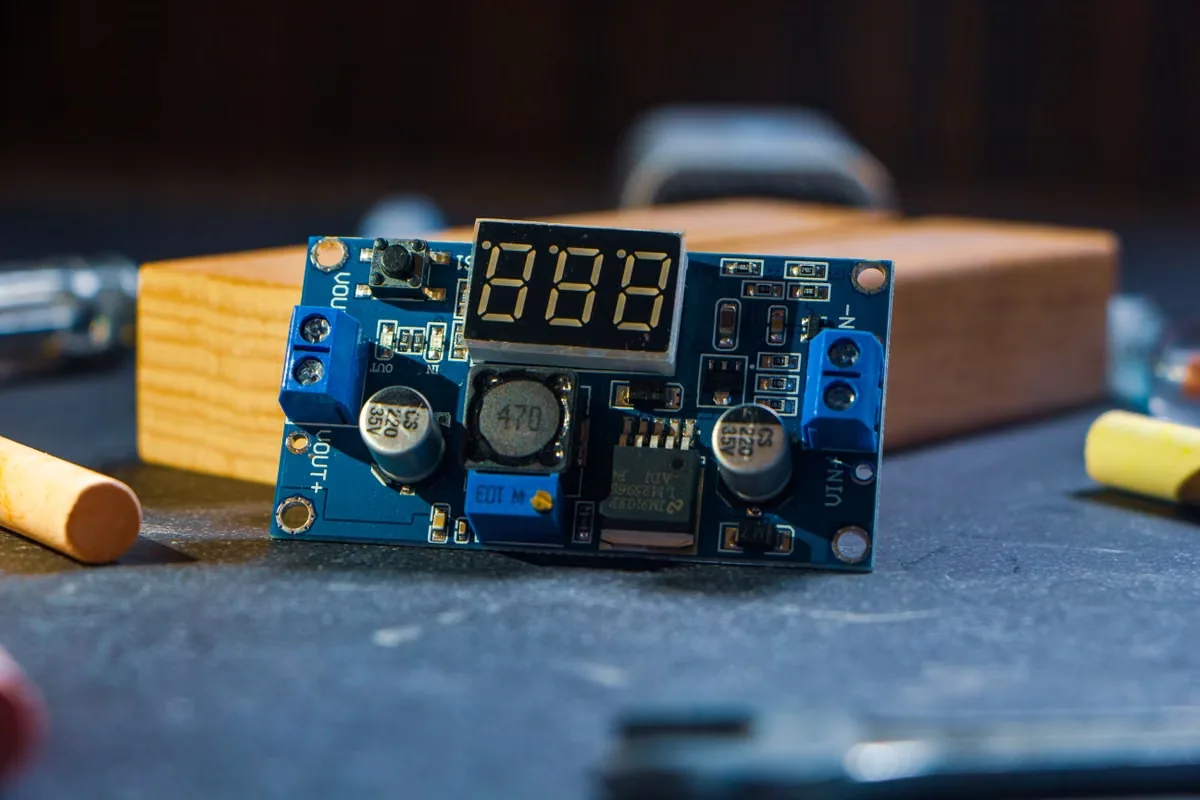
熱と電磁波吸収を、熱と干渉が同じ限られたスペースに存在する小型RF、ネットワーク、コンピューティングアセンブリに組み込みます。.
- 熱伝導およびEMI機能
- 周波数および配置の検討
- カスタム形状・厚さ
 05
05断熱パッド
保護が必要な基板、バスバー、センサー、筐体、または隣接部品の周囲に、熱的分離、絶縁間隔、クッション性を提供します。.
- 熱的・電気的分離
- 絶縁・難燃オプション
- カスタムゾーンと配置形状
 06
06サーマルシリコンクロス
深い隙間の充填よりも、耐突刺し性、寸法安定性、薄型絶縁が重視される場合に、強化キャリアによる補強と熱特性・電気特性を両立します。.
- 強化構造
- 厚みを管理した薄型インターフェース
- 打ち抜き加工による絶縁形状
 07
07グラファイト熱伝導パッド
厚く不均一なギャップを埋めるよりも面内熱伝導とホットスポットの均一化が重要な場合に、薄く軽量な層を介して集中した熱を横方向へ拡散します。.
- 高い面内熱拡散性能
- 薄型・軽量構造
- 導電性エッジおよび取り扱いレビュー
 08
08フルオロシリコーンサーマルパッド
油、燃料、クーラント、溶剤にさらされる熱インターフェースや、一般的なエラストマーでは特性が変化する可能性のある過酷なエンジンルーム内および産業環境に対応します。.
- 耐薬品性エラストマーの選択肢
- 絶縁材料によるギャップ充填
- 流体別適合性試験
選定時の優先事項
W/mKだけでなく、実際の界面に基づいて放熱パッドを選定する
バルク熱伝導率は、規定の試験方法に基づいて材料を比較するのに役立ちます。完成したアセンブリに存在するすべての接触界面、厚さ、圧力分布、経時劣化の影響が含まれるわけではありません。.
Gap and Compressed Thickness
Measure minimum, nominal and maximum gap across tolerance. Choose a supplied thickness that maintains contact without excessive material or force.
Hardness and Contact Pressure
Available clamping load, board strain, package fragility and housing stiffness determine how soft the pad must be.
熱インピーダンス
Evaluate the complete interface at a relevant thickness and pressure. A thin, conformable pad can outperform a higher-W/mK pad with poor contact.
Electrical and Environmental Fit
Confirm dielectric, flame, temperature, humidity, fluid, vibration, outgassing and service-life requirements.
Production Delivery Format
Include shape, liner, adhesive, orientation, packaging, placement method, inspection and annual volume in the material decision.
Thickness and Compression
Match Thermal Pad Thickness to the Entire Gap Range
The correct pad is not simply the closest catalog thickness to the nominal CAD gap. It must remain inside an acceptable compression window at the smallest and largest assembled gaps while protecting components and preserving useful contact.
 Use measured assembly evidence and tolerance—not a single nominal dimension—to define pad thickness.
Measure the Minimum Gap
Check whether the thickest component, housing bow, tolerance stack or fastener location could over-compress the pad and overload the board or package.
Measure the Maximum Gap
Confirm the thinnest component and widest housing condition still produce continuous contact after aging, vibration and fastener relaxation.
Define the Compression Window
Use supplier compression-deflection data and assembly force limits. Percent compression is not meaningful without the material curve and geometry.
Check Contact Area and Pressure Peaks
Ribs, screw bosses, package corners and local flatness can concentrate load. Review imprint or pressure evidence across the useful thermal footprint.
Avoid Stacking Thermal Pads
Stacked layers add interfaces, trap air, shift during assembly and create unpredictable thickness. Select one qualified construction where possible.
Recheck After Aging
Compression set, hardening, softening, vibration and housing movement can reduce recovery and contact pressure long after the first thermal test.
フォーマットの比較
Thermal Pads Versus Other Thermal Interface Materials
No TIM format is universally best. The choice changes with gap, flatness, pressure, assembly speed, repair, orientation and lifetime movement.
| 素材フォーマット | ベストフィット・インターフェース | 主な利点 | デザインの着眼点 |
|---|---|---|---|
| 熱伝導パッド | Defined component-to-housing or heat-sink gaps | Clean placement, controlled thickness and cushioning | Compression, hardness, tolerance and aging |
| 熱伝導グリス | Very thin, flat and well-clamped interfaces | 低い接着剤層と強力な表面濡れ性 | 排水、乾燥、音量調整およびサービス |
| 液体ギャップフィラー | Complex topography and variable component heights | Low assembly stress and automated dispensing | Slump, dispense repeatability, cure and rework |
| 相変化TIM | Thin processor and power-device interfaces | Dry handling followed by wetting in operation | Activation temperature, preload and cycling |
| サーマルアドヘシブ | Interface also requiring structural attachment | Bonding and heat transfer in one material | Cure, modulus, bond line, strength and repair |
アプリケーション市場
Thermal Pads for High-Demand Electronics Applications
Heat load is only one difference between markets. Gap variation, voltage, vibration, fluid exposure, service access, takt time and reliability profile change the best pad construction.

EV Batteries and Energy Storage
Bridge cells, modules, BMS electronics and cold plates while balancing dielectric safety, tolerance, vibration and flame requirements.
Explore EV Battery Materials
Power Electronics and Modules
Move heat from IGBT, MOSFET, converter and inverter assemblies while maintaining insulation and clamping integrity.
パワーエレクトロニクスを探索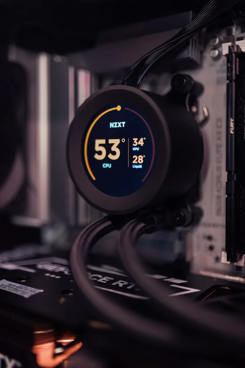
データセンターとAIサーバー
Control GPU, HBM, accelerator, VRM and networking temperatures through high power density and repeated service cycles.
Explore AI Server Cooling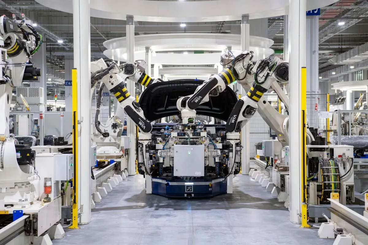
車載電子機器
Support ECUs, ADAS, infotainment and power modules through temperature cycling, shock, vibration and long qualification programs.
自動車電子機器の探索
通信・5G機器
Connect radios, power amplifiers, RRUs and network hardware to outdoor housings through weather, solar load and long field service.
Explore Telecom and 5G
LED照明
Move heat from LED boards and drivers while supporting optical stability, insulation and long outdoor or architectural service.
Explore LED LightingCustom Production Formats
Custom Die-Cut Thermal Pads From Prototype to Production
A production thermal pad is more than a material and outline. Geometry, cut method, adhesive, liner, orientation, packaging and inspection all affect whether the part can be placed cleanly and consistently.

Custom Shapes and Keep-Out Areas
Design around screws, ribs, connectors, busbars, sensors and electrical clearance while preserving the useful thermal footprint.
Adhesive and Surface Options
Compare natural tack, one-sided PSA, selective adhesive or non-tacky films against placement, thermal resistance and rework needs.
ライナー、タブ、配置補助具
プルタブ、スリット入りライナー、剥離性の制御、目視可能な方向表示により、伸び、汚染、配置ミスを低減します。.
シート、部品、アレイ、ロール
フルカット部品、ハーフカットアレイ、シートレイアウト、連続ロールを、手作業での組立、キッティング、または自動配置に適合させます。.
試作および初品レビュー
Check material construction, critical dimensions, liner behavior, part flatness, packaging and fit before scaling tooling and volume.
Production Change Control
Lock base material, thickness, adhesive, liner, cutting method, measurement practice and approved substitutions after qualification.
Engineering Brief
Information to Send for a Thermal Pad Recommendation
A complete brief reduces unsuitable samples and reveals whether the project truly needs a solid pad, another TIM format or a customized construction.
Review Material Selection and Testing熱源と冷却面
Component, package, power or heat load, contact area, heat sink, housing, spreader or cold-plate material.
Gap and Tolerance
Minimum, nominal and maximum assembled gap, flatness, roughness, ribs, bosses and keep-out geometry.
Pressure and Fragility
Fastener or clip load, allowable compression, board strain, package limit and movement during service.
Electrical and Environmental Needs
Working voltage, dielectric margin, flame target, ambient range, humidity, fluids, vibration and expected life.
組み立て工程
Manual or automated placement, liner preference, adhesive, inspection, rework, cleanliness and takt time.
Commercial Requirements
Drawing revision, sample quantity, target timing, forecast, annual volume, packaging and change-control expectations.
未然防止
Common Thermal Pad Selection Mistakes
A pad can produce an acceptable first temperature and still fail through assembly variation, mechanical stress, contamination or long-term loss of contact.
Choosing Only by Thermal Conductivity
W/mK does not include bond line, contact resistance, pressure or aging. Compare impedance under relevant conditions.
Compare Resistance and ImpedanceUsing a Pad That Is Too Thick
Extra thickness increases bulk resistance and can create excessive force, board bending or package stress.
Review Compression EffectsStacking Multiple Thermal Pads
Every added layer introduces another interface and more opportunities for air, shifting and inconsistent pressure.
Learn Why Pad Stacking Is RiskyIgnoring Compression Set and Aging
A pad may remain in position but lose recovery and useful contact after heat, cycling, vibration or fastener relaxation.
Review Thermal Pad FailuresAdding Adhesive Without Validation
PSA can aid placement but also adds thickness, stiffness, residue, aging risk and an additional thermal interface.
Read Die-Cutting Design TipsConfusing Conductive and Insulating Pads
A heat-conducting gap pad moves heat into a cooling structure. A thermal insulation pad protects a zone from heat. Define the function first.
Design a Custom Thermal Padエンジニアリングリソース
Thermal Pad Design and Validation Guides
Use focused engineering guides for questions that need more depth than a parent product category should carry.
Thermal Pad vs. Thermal Paste
Compare controlled gap filling with thin-interface wetting, assembly cleanliness, cycling and service.
Compare Pads and Pasteサーマルパッドが機能しなくなる理由
Review thickness, pressure, aging, contamination, cutting and application causes behind field problems.
Included in the failure section aboveThermal Pad Die-Cutting
Understand radii, holes, bridges, tolerances, liners, adhesive and delivery format for custom shapes.
Included in the failure section aboveExplore All Thermal Interface Materials
Place pads within the wider choice of grease, gap filler, phase-change and bonding materials.
Browse Thermal Interface MaterialsBrowse Electronics Application Markets
Start with the device, heat source, gap, environment and production constraints of the target system.
Explore Application MarketsBuild a Production-Ready Material Format
Connect formulation, converting, samples and process support with the actual manufacturing line.
Explore Customizationよくあるご質問
Thermal Pad FAQ
Final selection should be qualified in the real interface, pressure range, environment and production process.
熱伝導パッドにはどのような役割がありますか?
A thermal pad fills air gaps and surface irregularities between a heat-generating component and a cooler structure. It provides a more conductive path than air while offering controlled thickness and clean placement.
熱伝導率は高ければ高いほど常に良いのでしょうか?
No. Final thermal performance also depends on compressed thickness, contact resistance, pressure, surface flatness, coverage and aging. A conformable lower-W/mK pad can outperform a harder high-W/mK pad that makes poor contact.
How thick should a thermal pad be?
The pad should cover the complete assembled gap range with enough compression to maintain contact but without overstressing the component, board or housing. Measure minimum, nominal and maximum gaps rather than using nominal CAD alone.
How much should a thermal pad be compressed?
一律のパーセンテージはありません。サプライヤーの圧縮-たわみデータ、実際のパッド面積、利用可能なクランプ力、および部品の許容限界に基づき、安全な圧縮範囲を設定してください。.
Are thermal pads electrically insulating?
Many silicone gap pads are formulated for dielectric performance, but graphite and some functional materials can be electrically conductive. Verify the exact construction, compressed thickness, cut edges and assembly clearances.
Can thermal pads be stacked?
Stacking is generally less predictable because it adds interfaces, traps air and allows layers to shift. A single qualified thickness or custom construction is normally preferred.
Should a thermal pad have adhesive backing?
Adhesive can simplify retention and placement, especially on vertical surfaces. It can also add thermal resistance, stiffness, residue and rework difficulty, so natural tack or selective adhesive may be better in some assemblies.
When should thermal paste or liquid gap filler be used instead?
Thermal paste suits very thin, flat and clamped interfaces. Liquid gap filler suits complex topography, variable heights and low-stress automated dispensing. Pads suit defined gaps, clean placement and repeatable solid-part handling.
Can Haktak provide custom die-cut thermal pads?
Haktak can support material selection and custom formats such as sheets, individual parts, kiss-cut arrays or rolls with application-specific shape, liner and adhesive requirements.
What information is needed for a sample?
Share the drawing, gap range, contact area, heat target, pressure limit, voltage, environment, placement method, reliability plan, sample quantity and expected production volume.
Start With the Complete Interface
Send the Gap, Pressure, Heat Load and Production Process
Haktak can help compare thermal pad materials, thicknesses, custom shapes and delivery formats for electronics prototypes and production assemblies.