
Semiconductor and Electronics Assembly Materials
Semiconductor and Electronics Assembly Materials for Reliable Packaging
Select underfill, coating, bonding, encapsulation and thermal materials around package geometry, substrate compatibility, precision dispensing, cure conditions, ionic cleanliness and long-term reliability.

議会内で
Map Every Semiconductor and Electronics Assembly Interface
Fine-pitch packaging and dense electronics use different materials at different zones. The correct choice starts with the component, substrates, gap, protection function and production process.
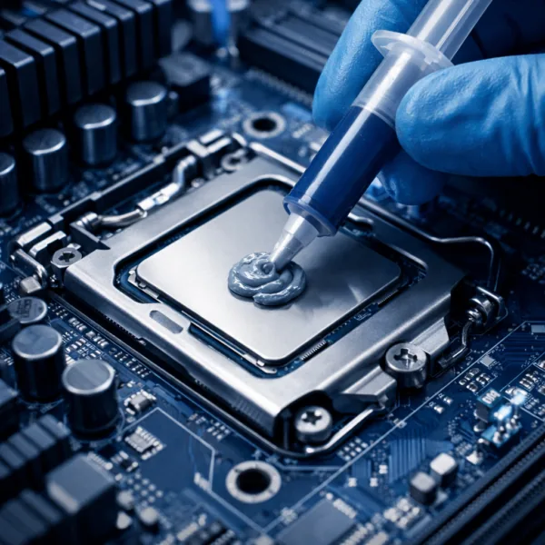
Underfill for BGA, CSP and Flip-Chip Packages
Control capillary flow, fillet shape, voiding and cured stress around fine-pitch interconnects while matching board materials and the permitted cure profile.
Explore Electronic Assembly Adhesives →
Package, Heat Spreader and Cooling Interfaces
Reduce interface resistance around processors, accelerators and modules while controlling bond-line thickness, pressure, cleanliness and rework.
View Thermal Interface Materials →
Coating, Sealing and Selective Encapsulation
Protect boards, wire bonds, connectors and sensitive components against moisture, contamination and vibration without creating excessive cure stress.
Read the Potting Compound Guide →マテリアルファミリー
Choose Semiconductor Assembly Adhesives by Function
Start with the job the cured material must perform. Chemistry, viscosity and cure method should follow the package geometry, substrates, stress limit and production window.
Semiconductor Underfill Adhesives
Reinforce solder joints and redistribute stress beneath BGA, CSP and flip-chip packages.
- Capillary or no-flow process
- Low voiding and controlled fillet
- CTE and modulus balance
UV-Curable Coating Materials
Protect accessible board areas with rapid cure and precise process control while accounting for shadow zones.
- Fast on-demand cure
- Selective coating capability
- Inspection-friendly application
Structural Electronics Assembly Adhesives
Attach housings, substrates, stiffeners and components while absorbing mechanical and thermal expansion stress.
- Bond strength and toughness
- Dissimilar substrate adhesion
- Controlled cure and open time
Sealing and Encapsulation Materials
Protect electronics from humidity, dust, chemicals and vibration through local sealing or cavity filling.
- Flexible environmental barrier
- 誘電保護
- Repair and cure considerations
Silicone-Free Thermal Interfaces
Transfer heat near sensitive contacts, optics and coating operations where siloxane migration is a concern.
- クリーンコンタクト要件
- Pad or custom die-cut format
- 互換性検証
Thermally Conductive Assembly Adhesives
Combine mechanical attachment with heat transfer for spreaders, sensors, modules and cooling components.
- ボンディング+サーマルパス
- 1K or 2K process options
- Modulus and rework balance
Material Comparison
Compare Underfill, Coating, Bonding and Encapsulation Materials
Materials that appear similar before cure can produce very different flow, stress, protection and repair outcomes in the finished electronic assembly.
| Material Function | Best-Fit Assembly Zone | Primary Value | デザインの着眼点 |
|---|---|---|---|
| Capillary underfill | Beneath BGA, CSP and flip-chip packages | Interconnect reinforcement and stress distribution | Flow distance, voids, fillet, cure and rework |
| Conformal coating | PCB surfaces, traces and exposed component areas | Thin moisture and contamination protection | Coverage, shadow zones, masking, cure and inspection |
| Structural adhesive | Housing, substrate, stiffener, component or module bond | Mechanical attachment and stress transfer | Adhesion, modulus, open time, cure and disassembly |
| 封止材またはポッティング | Local component zone or complete electronic cavity | Environmental, dielectric and mechanical protection | Exotherm, shrinkage, voids, mass and repair |
| Thermal interface | Package, spreader, heat sink or enclosure interface | Lower contact resistance and heat transfer | Thickness, pressure, cleanliness and pump-out |
| サーマルアドヘシブ | Heat spreader, sensor, module or cooling component | 接合と熱伝導を一つの工程で | Bond line, cure stress, strength and rework |
選択ワークフロー
Build an Electronic Assembly Material Brief in Five Steps
A useful brief links component geometry and substrates to dispensing, cure, contamination and reliability requirements before material samples are ordered.
Define the Assembly Function
Identify whether the material must underfill, coat, seal, bond, encapsulate or transfer heat.
Map Package and Substrates
Record component dimensions, pitch, stand-off, surface finish, board materials and sensitive regions.
Set the Dispense Window
Define viscosity, flow distance, bead or dot geometry, open time, keep-out zones and takt time.
Choose the Cure Process
Confirm UV, heat, moisture or two-component cure, maximum temperature and shadow limitations.
Validate Assembly Reliability
Test adhesion, voiding, ionic cleanliness, thermal cycling, moisture, vibration and rework.
エンジニアリング変数
What Should Be Specified Before Semiconductor Assembly Sampling?
Sample selection improves when the material is evaluated with the actual package, substrates, dispense equipment and cure profile. Share target ranges when the line is still being developed.
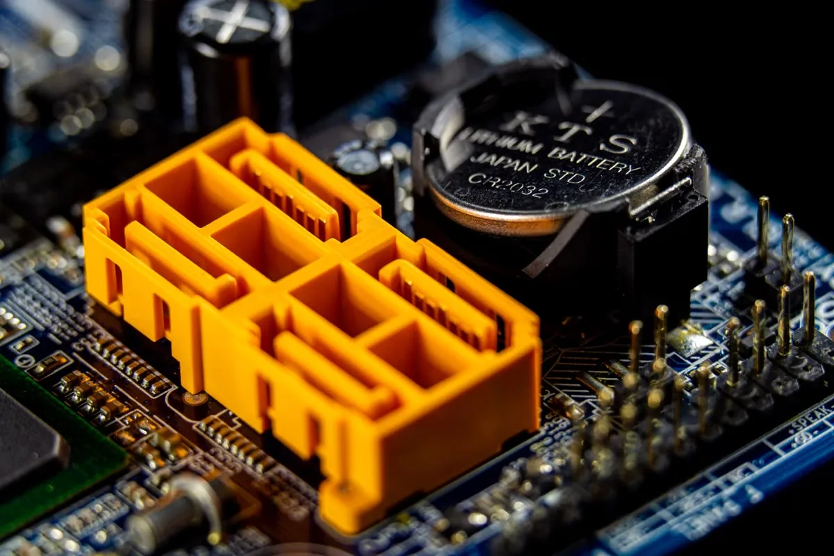 The finished process—not liquid properties in isolation—defines assembly performance.
Package Geometry
Package type, pitch, stand-off, flow distance, fillet target, gap, keep-out zones and component fragility.
Substrates and Surface Finish
Silicon, mold compound, solder mask, copper, ceramic, glass, plastics, metals and surface treatment.
Dispensing Requirements
Viscosity, thixotropy, needle or jetting method, bead geometry, flow time, pot life and equipment limits.
状態異常の治療
Maximum temperature, UV access, moisture exposure, mix ratio, cure time and allowable process energy.
Cleanliness and Compatibility
Outgassing, ionic contamination, siloxane sensitivity, corrosion risk and compatibility with nearby materials.
Reliability and Rework
Thermal cycling, humidity, vibration, drop or shock, operating life, inspection and repair expectations.
未然防止
Prevent Semiconductor Adhesive and Coating Failures
Initial adhesion or cure is not enough. Assembly defects often come from flow, trapped air, contamination, cure mismatch and stress after environmental cycling.
Incomplete Underfill or Entrapped Voids
Viscosity, package stand-off, dispense path and substrate temperature can prevent complete capillary flow.
Review Low-Modulus Flow Behavior →Excessive Exotherm or Cure Stress
Large volumes and rigid systems can generate heat, shrinkage and stress around packages, solder joints and boards.
Understand Epoxy Potting Behavior →Outgassing and Sensitive-Surface Contamination
Volatile residues can affect optics, contacts, vacuum processes, bonding and long-term surface cleanliness.
Review Outgassing Risks →Poor Bonding to Mixed Substrates
One adhesive may wet metal well but perform poorly on solder mask, engineering plastic or treated glass.
Review Fast-Bonding Adhesive Limits →Coating Gaps and Moisture Paths
Masking, sharp edges, connectors and shadow regions can create discontinuities in environmental protection.
Plan Moisture and Dust Protection →CTE Mismatch and Delamination
Rigid bonds across dissimilar materials can accumulate peel and shear stress through temperature cycling.
Compare Flexible Adhesive Behavior →Assembly Platforms
Match Materials to Semiconductor Packaging and Electronics Assembly
Package architecture, board density, service environment, qualification level and volume determine the correct balance of flow, cure, stress and protection.
Flip Chip, BGA and Accelerator Packages
- Fine-pitch underfill flow
- Low stress and low voiding
- Thermal interface cleanliness

Automotive Modules and Sensor Electronics
- Thermal cycling and vibration
- Moisture and chemical protection
- Qualification-driven processing
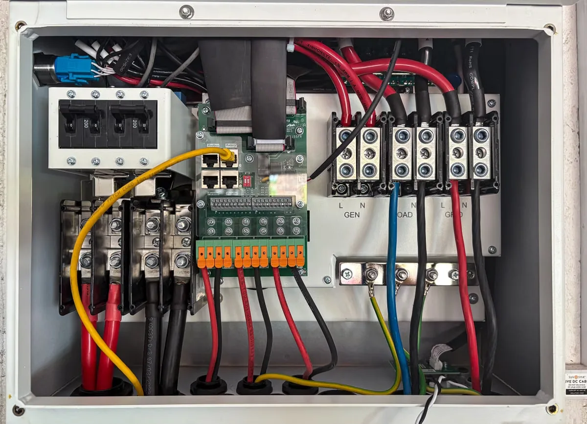
Industrial Controls and Power Boards
- Selective coating and potting
- Rugged environmental exposure
- Repair strategy and long life
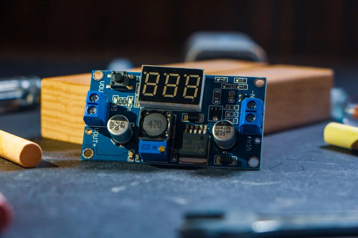
Consumer, LED and Compact Electronics
- Fast cure and short takt time
- Precise low-volume dispensing
- Thin, compact assemblies
検証計画
Validate Semiconductor Assembly Materials in the Real Process
Material data narrows candidates. Process and assembly testing confirm whether flow, cure, adhesion, cleanliness and protection remain stable in the actual package and production line.
材料の選定と試験を見る →Flow and Voiding
Measure capillary travel, fillet shape, trapped air and coverage across real package geometry.
Adhesion and Cohesion
Test relevant substrates before and after cure, moisture, heat exposure and thermal cycling.
Cure Verification
Confirm complete cure, shadow regions, hardness, conversion and process tolerance.
Cleanliness and Outgassing
Evaluate ionic residue, volatile loss, corrosion and contamination-sensitive surfaces.
環境信頼性
Run thermal cycling, humidity, vibration, shock, high-temperature storage and application tests.
Inspection and Rework
Define visual, optical or X-ray inspection criteria and practical repair or removal procedures.
プロトタイプから本番へ
Scale Precision Dispensing From Prototype to Production
Haktak can support formulation and process fit. Share component drawings, substrates, dispense equipment, cure limits, quality criteria and annual volume early in development.
Viscosity and Flow Tuning
Adjust flow, thixotropy, slump, jetting behavior and fillet control around the package geometry.
Cure Process Alignment
Match UV, thermal, moisture or two-component cure to temperature limits and takt time.
調剤支援
Align packaging, needle or jet parameters, bead path, shot size, pot life and equipment cleaning.
試作品
Compare chemistry, modulus, flow and cure ranges before process qualification and volume release.
エンジニアリングリソース
Semiconductor and Electronics Assembly Material Guides
Use these technical guides to compare adhesive behavior, thermal performance, contamination risk and process options before qualification.
熱伝導性接着剤とは何ですか?
Understand how bonding, thermal transfer, cure and modulus interact in electronic assemblies.
サーマル接着剤ガイドを読む →Thermally Conductive Structural Adhesives
Review attachment, heat flow and mechanical reliability for demanding electronic modules.
Review Structural Adhesive Design →What Is a Thermal Adhesive?
Compare thermal adhesives with pads, grease and conventional structural materials.
Compare Thermal Material Formats →Silicone-Free Thermal Solutions
Consider contacts, optics, coating and downstream bonding where silicone migration matters.
Review Silicone-Free Options →Thermal Conduction in Electronics
Connect heat sources, interfaces and cooling structures across complete electronic assemblies.
Read the Thermal Design Guide →Browse Haktak Assembly Materials
Review thermal interface, adhesive, sealing and encapsulation product families and grades.
すべての製品を見る →よくあるご質問
Semiconductor Assembly Adhesive FAQ
Final selection should be validated with the real package, substrates, dispense method, cure profile and reliability plan.
What is underfill used for in semiconductor assembly?
Underfill fills the space beneath packages such as BGA, CSP and flip chip to reinforce solder joints and redistribute stress caused by thermal expansion, mechanical shock and board flexing.
How do I choose an underfill adhesive?
Start with package stand-off, flow distance, pitch, substrates, dispense process, cure limit, required modulus, CTE, glass-transition behavior, void target, reliability testing and rework needs.
What is the difference between coating and encapsulation?
Conformal coating creates a thin protective layer over board surfaces. Encapsulation or potting fills a larger local zone or cavity and usually provides greater mechanical and dielectric protection, but adds mass and complicates repair.
When should a low-outgassing adhesive be considered?
Consider low-outgassing materials near optics, sensors, precision contacts, vacuum processes and contamination-sensitive packages. Test volatile behavior and surface compatibility under the real operating conditions.
Can one adhesive provide structural bonding and heat transfer?
Yes. Thermally conductive adhesives can attach components or spreaders while conducting heat, but bond-line thickness, cure, modulus, adhesion, thermal cycling and rework must be evaluated together.
ハクタックがおすすめをするためには、どのような情報が必要ですか?
Share package and substrate details, gap or stand-off, dispense equipment, flow target, cure limits, cleanliness requirements, reliability tests, takt time, rework expectations and annual volume.
Start With the Package and Process
Send the Geometry, Substrates, Dispense Path and Cure Limits
Haktak can help compare underfill, coating, structural bonding, encapsulation and thermal materials for semiconductor packaging and precision electronics assembly.