
サーマルパッドは、バッテリーマネジメントシステムにおいて、BMS 電子部品から金属筐体、ヒートスプレッダー、コールドプレートなどの冷却面へ熱を移動させるために使用されます。発熱部品と冷却構造の間にある空気層を埋めます。優れたサーマルパッドは接触性を高め、局所的なホットスポットを低減し、基板温度をより安定させます。.

主な発熱源には、セルバランシング抵抗、保護用MOSFET、電流検出部品、電力コンバータ、ゲートドライバ、通信回路、BMSプロセッサなどがあります。最も高温になる部位は、アーキテクチャと動作モードによって異なります。パッシブバランシングでは、抵抗バンク周辺に熱が集中することがあります。充電および放電電流によって、保護デバイスやシャントが発熱する場合があります。また、高電圧バッテリーパックでは、限られた通気しかない温度の高い筐体内にBMSが配置されることもあります。.
適切なBMS放熱パッドは、単にW/mK値が最も高い製品というわけではありません。エンジニアは、最終接着層厚さ、圧縮荷重、絶縁破壊強度、表面接触性、パッド硬度、使用温度範囲、難燃要件、経時劣化も考慮する必要があります。パッドは、PCBを曲げたり、はんだ接合部に荷重をかけたり、近傍のセンサーが測定する温度を変化させたりすることなく、電子機器を冷却できなければなりません。.
What Does a Battery Management System Need to Keep Cool?
A battery management system measures cell voltage, pack current, and temperature. It estimates state of charge and state of health. It also controls balancing, contactors, charging limits, discharge limits, and fault responses. Accurate data is central to these decisions. Analog Devices describes BMS accuracy and stability across time, temperature, and operating conditions as essential to reliable cell monitoring in its overview of battery management system longevity.
A BMS may consume far less power than the battery it controls, but its heat is concentrated on a small PCB. The board may sit inside a sealed metal pack with little natural airflow. Nearby cells, busbars, contactors, and power electronics may raise the local ambient temperature. This makes a modest component loss more difficult to remove.
Cell-balancing resistors and BMS board heat dissipation
Passive balancing burns excess cell energy as heat. The resistor value, balancing current, number of active channels, and duty cycle determine the total loss. Several resistors can operate together. Their heat can raise the temperature of the PCB, the battery monitor IC, and nearby connectors.
The thermal pad does not need to cover every resistor directly. In some layouts, copper planes spread heat to a defined pad area on the back of the PCB. That pad then conducts heat into the enclosure. In other designs, a pad contacts the tops of a resistor bank. Both approaches can work, but they create different electrical and mechanical risks.
MOSFETs, shunts, and protection components in a BMS
Protection MOSFETs can generate conduction and switching loss. Current shunts dissipate power according to the square of current multiplied by resistance. DC/DC converters, linear regulators, gate drivers, and precharge circuits add further heat. These sources may operate only in certain modes, so a steady idle test can miss the worst condition.
If MOSFETs dominate the loss, use a pad that can maintain contact over package and PCB tolerance without overstressing the leads or solder joints. The selection logic in MOSFET用サーマルパッド:エンジニア向け選定ガイド also applies to BMS protection stages, especially when several packages share one enclosure surface.
Battery monitor ICs, processors, and isolated communication devices
Battery monitor ICs and processors often have lower power loss than balancing components or MOSFETs. They can still be sensitive to local temperature. Excessive temperature may reduce electrical margin, increase drift, or shorten component life. Thermal gradients across the board can also complicate temperature compensation.
Cooling these components should be deliberate. A large pad covering the entire board may couple a precision circuit to a hot enclosure zone. A smaller zoned pad can give better control. The goal is not to make every component the same temperature. The goal is to keep critical parts within their limits while preserving accurate sensing.
BMS Thermal Pads Are Not a Complete Battery Cooling System

「バッテリー熱管理」という表現は、多くの場合、空冷、液冷、冷媒、ヒートパイプ、相変化システムなどによってセルやモジュールの温度を制御することを指します。BMS基板上のサーマルパッドは、より限定的な役割を担います。電子制御部から熱を逃がし、バッテリーパックの特定の表面間の熱結合を補助することはできますが、適切に設計されたセル冷却システムの代わりにはなりません。.
NRELの取り組み battery thermal management design modeling emphasizes both operating temperature and temperature uniformity across cells and modules. Those pack-level goals require a full thermal design. BMS thermal pads support that design by keeping monitoring and control electronics reliable. They should not be presented as a safeguard that can stop thermal runaway by themselves.
This distinction matters during root-cause analysis. If cells are running hot because coolant flow is poor, adding a higher-conductivity pad to the BMS board will not solve the cell problem. If the BMS processor resets because balancing resistors heat a sealed control compartment, a targeted board-to-housing pad may be effective.
How Thermal Pads Improve BMS Heat Dissipation
空気は、充填材入りの熱伝導インターフェース材料と比べて熱伝導性が低いものです。実際の部品、PCB、筐体の表面は完全に平坦ではありません。柔軟なインターフェースがなければ、接触するのは凸部だけになります。残った空間は、断熱性のある空気層として機能します。.
サーマルギャップパッドは、組み立て時の圧力によって変形します。表面の凹凸に追従し、高さのばらつきを橋渡しします。これにより、部品またはPCBからパッドを通って、より大きな冷却構造へ熱を移動させることができます。その構造には、BMSカバー、アルミニウム製ベースプレート、鋳造ハウジング、バスバー用ヒートスプレッダ、または電子部品から絶縁されたコールドプレートなどがあります。HakTakの 熱伝導パッド は、この種の部品-ハウジング間またはPCB-ハウジング間の熱経路を想定しています。.
The complete heat path might be:
- Semiconductor junction or resistor body
- Component package and solder connection
- PCB copper and dielectric layers
- BMS thermal pad
- Metal housing or heat spreader
- Ambient air or pack cooling circuit
Every layer adds thermal resistance. A pad can improve one weak interface, but it cannot compensate for a poor copper layout, an undersized housing, or insufficient external cooling. This is why thermal interface selection should begin after the major heat path is understood.
How to Choose a Thermal Pad for a BMS Board
The best thermal pad for a BMS is the thinnest compliant material that maintains contact across production tolerance, keeps component temperatures within target, provides the required electrical isolation, and stays mechanically stable for the product life.
| 選択因子 | BMSについて確認すべき事項 | 無視した場合に起こりやすい故障 |
| 熱負荷 | 部品および動作モード別の損失 | バランシング時または大電流時にのみホットスポットが発生 |
| ギャップ範囲 | 組み立て後のギャップの最小値と最大値 | 一方のユニットでは接触せず、別のユニットでは過大な力がかかる |
| 熱インピーダンス | 該当する圧力および厚さでのデータ | W/mKの高いパッドでも、システム温度が期待外れになる |
| 圧縮力 | 公差限界での圧力 | PCBの反り、はんだ損傷、パッケージ荷重 |
| 電気絶縁 | 絶縁破壊電圧および絶縁抵抗 | 接地または通電中の金属筐体への短絡 |
| 硬度および追従性 | 部品および基板のばらつきに対する接触性 | 空気溜まりおよび不均一な圧力 |
| 温度範囲 | 連続使用およびサイクル運転の限界 | 硬化、ひび割れ、クリープ、またはタックの喪失 |
| 可燃性 | 製品および規制要件 | 材料がパックレベルの安全性認証試験に不合格となる |
| 信頼性 | 熱・湿度・振動・圧縮による経時劣化 | 使用期間に伴う接触性能の低下 |
| 製造 | ダイカット、ライナー剥離、貼り付け、リワーク | 位置ずれ、破れ、汚染、気泡の混入 |
パッドのデータシートではなく、まずBMSの電力マップから始めます
重要なすべての動作モードにおけるコンポーネント損失を計算または測定します。充電、放電、バランシング、スリープ、ウェイクアップ、フォルト、通信状態を含めます。複数のバランシングチャネルが動作している一方で、パック筐体がすでに高温になっているケースを確認します。MOSFET抵抗、シャント抵抗、コンバータ効率、電源電圧の公差を含めます。.
熱電対、測温抵抗体、校正済み赤外線測定、またはパッケージ温度の推定値を、適切に使い分けます。赤外線画像は高温領域の特定に有用ですが、放射率や金属表面からの反射によって誤差が生じる可能性があります。重要な箇所は接触式センサーで確認してください。.
冷却面温度を定義する
パッドは熱を別の表面へ移動させるだけです。その移動先は熱源より低温に保たれていなければなりません。同じ最悪条件の動作モード中に、筐体温度を測定またはモデル化します。ハウジングが近接するセルまたはコンタクタによって加熱される場合、ヒートシンクとして機能しにくくなる可能性があります。.
コールドスタート時やパックの急速加熱時には、熱経路が逆向きになることもあります。熱結合によって、筐体からBMSの電子部品が温められる場合があります。パックが広い周囲温度範囲で動作する場合は、両方向を確認してください。.
BMS用サーマルパッドの熱伝導率と熱インピーダンス
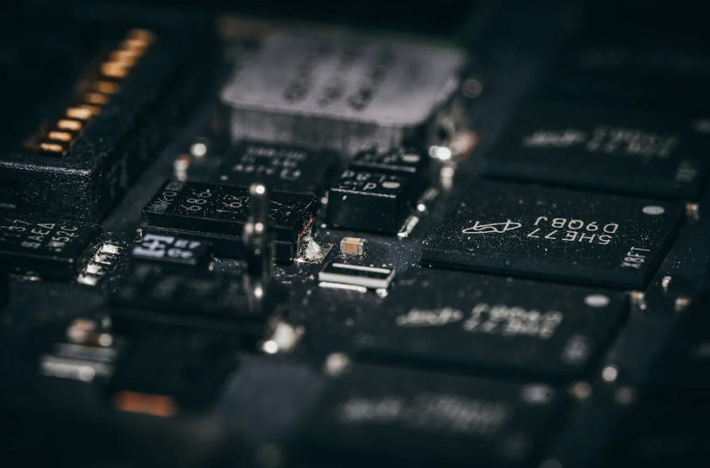
熱伝導率はW/mKで示され、バルク材料内部を熱がどれだけ容易に移動するかを表します。熱インピーダンスは、規定条件下における特定の界面構造の熱抵抗を表します。BMS基板では、厚さと接触の影響が含まれるため、熱インピーダンスのほうが通常、エンジニアが重視する結果に近くなります。.
均一な層として単純化した場合、熱抵抗は次の式で表されます:
R = t / (k x A)
ここです、, t 圧縮後の厚さを表します。, k 熱伝導率は、 A 有効熱伝達面積を表します。この式は方向性を把握するのに役立ちますが、実際のギャップパッドでは両面に接触熱抵抗も生じます。柔軟性、圧力、タック性、平坦度、粗さが、これらの接触部に影響します。.
高いW/mK値がBMSの冷却性能向上を保証しない理由
A 6 W/mK pad can perform worse than a 3 W/mK pad if the first product is much thicker or too hard to make good contact. High filler loading can increase conductivity while also increasing hardness. The stiffer pad may leave voids around small packages or transmit too much force into the board.
HakTakの関連記事は なぜ高いW/mKが必ずしも優れた冷却性能を意味するとは限らないのか このトレードオフを実用的な観点から説明しています。BMSを選定する際は、カタログ上の熱伝導率だけで順位付けするのではなく、最終ギャップ、圧力、面積、温度を同一条件にして候補を比較してください。.
比較可能な熱試験データを使用する
ASTM D5470 定常熱インピーダンスおよび熱伝導性電気絶縁材料の見かけの熱伝導率の測定を対象とします。この方法は界面材料の比較に有用ですが、ASTMは、理想化された熱流条件が実際の用途の大半を直接再現するものではないと指摘しています。したがって、サプライヤーのデータは材料のスクリーニングに活用し、その後にアセンブリ試験を実施してください。.
バルク熱伝導率と界面全体の性能の違いについては、以下でさらに詳しく説明しています TIM選定における熱伝導率と熱インピーダンス. .見積もりを確認する際は、各サプライヤーに試験方法、試料厚さ、圧力、温度、および報告値が標準値か保証値かを確認してください。.
バッテリーマネジメントシステム用サーマルパッド厚さの選定方法
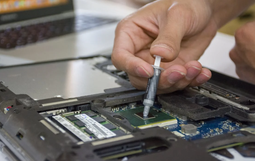
パッド厚さは、機械公差の積み上げから決定してください。対象部品またはPCB表面と冷却面との距離を測定します。部品高さ、はんだ厚さ、PCBの反り、筐体の平面度、締結部品の位置、ガスケットの圧縮、パッド公差、および組立ばらつきを含めてください。.
適切な公称パッドは通常、最大ギャップでも接触を維持できる、入手可能な最も薄い選択肢です。厚みを増やすと熱抵抗が増加します。また、最小ギャップで変形させる必要がある材料の量も増加します。.
公差の両端におけるBMS熱伝導パッドの圧縮率を計算する
圧縮率は次のように推定できます:
圧縮率 (%) = (初期 パッド 厚さ – 最終ギャップ) / パッドの初期厚さ x 100
Suppose a nominal 2.0 mm pad must fill a gap from 1.5 to 1.8 mm. At the 1.8 mm maximum gap, compression is 10%. At the 1.5 mm minimum gap, compression is 25%. The pad must maintain useful contact at 10% while staying within the board’s force limit at 25%.
Repeat this calculation at several locations if one pad covers multiple components. A cover can tilt, and a PCB can bow between fasteners. One corner may see little compression while another is overloaded.
HakTak’s guide on how to select thermal pad thickness for electronics provides a fuller tolerance method. Use the compressed bond line rather than nominal sheet thickness in thermal calculations, as explained in ボンドラインの厚さが熱性能に与える影響.
Avoid using thick pads to hide an uncontrolled enclosure design
A thick, soft pad can absorb large dimensional variation, but it carries a thermal penalty. Before accepting a 4 or 5 mm interface, check whether a formed metal boss, local heat spreader, board support, or housing change can reduce the gap. A small mechanical change may improve cooling more than a costly jump in thermal conductivity.
Large unsupported pads can also sag, shift, or make placement harder. If a wide gap cannot be reduced, compare the available サーマルインターフェースマテリアル and consider whether thermal putty or a cured gap filler fits the tolerance and production process better. HakTak’s comparison of thermal putty vs thermal pads for uneven gaps can help frame that decision.
How Much Compression Does a BMS Thermal Pad Need?
Compression improves contact by pushing the pad into surface texture and height variation. Too little compression leaves air pockets. Too much compression increases force, deforms the board, and may damage the pad or components.
There is no universal compression percentage. The correct range comes from the product’s pressure-deflection data and the mechanical limits of the assembly. Two pads with the same Shore 00 hardness can produce different forces because thickness, reinforcement, filler loading, and viscoelastic behavior differ.
Protect the PCB, solder joints, and sensor connections
BMS boards can be long and thin. A large pad under a cover creates force across a wide area. Even modest pressure can produce a large total load. Board deflection can strain solder joints, connectors, cell-tap terminals, isolation components, and conformal coating.
Very soft pads are often useful when multiple BMS components share one metal cover. They follow package height variation with less force. A harder pad may be easier to handle, but it can bridge over low components and concentrate load on tall ones. The article ソフト対ハードサーマルパッド:どちらが良い? explains how to balance conformability and assembly control.
Check stress relaxation after the BMS is assembled
Gap pads are viscoelastic. Their force changes after clamping and thermal exposure. Some initial stress relaxes, which can protect the board, but enough contact pressure must remain for heat transfer. Compression set can also prevent the pad from following movement during service.
Use supplier curves and aged samples. Do not assume the installation force remains constant. HakTak’s guide to サーマルパッドの圧縮率 shows how minimum and maximum gaps should be checked together rather than applying one nominal percentage to every unit.
Electrically Insulating Thermal Pads for BMS Boards
BMS electronics may operate at pack potential or across isolated domains. The metal enclosure may be grounded, floating, or connected to another electrical node. A thermal interface that touches both the board and enclosure must fit the insulation architecture.
Many silicone and non-silicone gap pads use electrically insulating ceramic fillers. However, not every thermal pad is an electrical insulator. Some interface materials contain conductive graphite or metal. Always review the exact construction and test data.
Dielectric strength is not the only insulation requirement
Dielectric strength is commonly expressed in kV/mm. Breakdown voltage applies to a specimen of a defined thickness under a stated test. The system also needs adequate insulation resistance, creepage, clearance, puncture resistance, and fault margin. Sharp component leads, housing burrs, screw bosses, and particles can weaken a soft interface.
If the pad serves as functional or reinforced insulation, involve the safety and compliance team early. Do not divide a catalogue kV/mm value by working voltage and treat the result as a complete insulation design. HakTak’s guide to 電気絶縁性サーマルパッド covers breakdown voltage, thickness, construction, and application risk in more detail.
Reinforced thermal pads for battery electronics
Fiberglass or dielectric-film reinforcement can improve handling and puncture resistance. It can also reduce conformability or increase the pressure required for contact. Reinforcement should be evaluated as part of the complete pad, not added only because the BMS carries high voltage.
For direct contact with soldered leads or sharp features, consider a smooth insulating barrier or a controlled keep-out zone. A thermal pad should not be expected to absorb uncontrolled metal edges throughout vibration and service life.
Thermal Pads and BMS Temperature-Sensing Accuracy

Temperature sensing is one of the BMS’s core functions. TI notes that battery management systems monitor cell voltage, current, and temperature for health and safety, and its application brief on thermistors for BMS thermal protection discusses temperature measurement within the wider control system.
A thermal pad can improve electronic reliability while also changing the temperature field around sensors. This is not always beneficial. A pad placed under a thermistor may conduct enclosure temperature into the sensor. A pad near a balancing resistor may spread resistor heat toward a measurement point. Either effect can make the reading less representative of the target cell or component.
Keep cell-temperature sensors thermally tied to the cells
If a sensor is intended to measure a cell, its dominant thermal path should lead to that cell. Avoid allowing a BMS board pad to couple the sensor more strongly to the housing. Review the sensor location, adhesive, lead conduction, airflow, copper area, and nearby heat sources.
The pad layout may need openings around thermistors or precision references. Zoned thermal pads can cool power components while leaving sensing regions less coupled. Validate the sensor reading during fast charge, discharge, balancing, cold soak, and changing coolant temperature.
Account for self-heating near current measurement circuits
Current-sense resistors and integrated sense elements generate heat. Analog Devices explains that sense-resistor self-heating can affect temperature readings depending on current, package, airflow, and thermal coupling. A thermal pad may reduce that local rise, but it may also change the calibration relationship.
Perform calibration and accuracy checks in the final mechanical assembly. A bare-board laboratory result may not remain valid after the PCB is pressed against a metal housing through a gap pad.
Silicone vs Non-Silicone Thermal Pads for Battery Management Systems
Silicone elastomer pads are common in battery electronics because they can combine softness, temperature resistance, electrical insulation, and a broad range of thicknesses and conductivities. They are a strong default when the product has no specific silicone restriction.
Non-silicone pads use another polymer matrix. They may be selected when silicone oil migration, volatile siloxanes, coating compatibility, optical contamination, or a customer material restriction matters. This is more likely when the BMS shares an enclosure with sensitive contacts, optical sensors, relays, or manufacturing processes that control silicone contamination.
Neither chemistry is automatically better for heat transfer. Compare thermal impedance, compression force, temperature rating, dielectric performance, outgassing, and long-term aging. HakTak’s silicone vs non-silicone thermal pad comparison explains how low-bleed silicone grades and verified silicone-free materials fit different contamination risks.
Where Should Thermal Pads Be Placed on a BMS?
Pad placement should follow the measured heat map and the mechanical load path. Common arrangements include pads between top-side components and the metal cover, pads between the back of the PCB and a baseplate, or local pads on power devices and balancing resistor zones.
| BMSパッド 場所 | Main Benefit | Main Design Concern |
| Over balancing resistors | Direct removal of concentrated balancing heat | Force on resistor bodies and solder joints |
| Over MOSFET packages | Short path to metal cover | Package height tolerance and electrical potential |
| Under PCB hot zone | Spreads load over copper-backed area | PCB dielectric and copper layout limit heat flow |
| Over DC/DC or regulator section | Reduces local regulator temperature | Nearby transformer or inductor height variation |
| Full-board pad | Simple placement and broad contact | High total force and unwanted sensor coupling |
| ゾーン分割型マルチパッドレイアウト | 熱源と許容荷重に適合 | 部品番号と組立手順が増える |
表面側部品の冷却と裏面PCB冷却
表面側冷却はパッケージからカバーまでの短い経路を形成しますが、部品に直接荷重がかかります。裏面冷却は、PCBにサーマルビアと銅箔プレーンがある場合、荷重をより安全に分散できます。また、放熱経路にPCBスタックが加わります。.
Use thermal simulation and measurement to compare both options. A back-side pad may outperform a direct pad if it has larger area, thinner bond line, and better mechanical support. A direct top-side pad may win when the package has a suitable flat surface and controlled height.
One large pad vs several local BMS thermal pads
One large pad simplifies the bill of materials. It can also create uneven compression over mixed component heights. Several local pads let engineers tune thickness and hardness by zone. They increase placement work and the chance of assembly error.
For high-volume production, die-cutting several features into one carrier can combine zoned contact with one placement step. Verify liner release, dimensional stability, narrow-wall strength, and pick-and-place behavior before freezing the design.
Thermal Pad Requirements by BMS Architecture
Centralized BMS thermal pad selection
A centralized BMS brings monitoring and control functions onto one main board. Heat can be concentrated around balancing banks, power supplies, contactor drivers, processors, and communication interfaces. The board may need several pad zones with different thicknesses.
Large boards are more sensitive to flatness and cover tolerance. Total compression force can become significant. Board supports and fastener placement should be designed together with the pad layout.
Distributed and modular BMS cooling
A distributed BMS places cell-monitoring electronics close to modules or cells. Each board may generate less heat, but it lives closer to cell temperature and may have limited enclosure volume. Pad placement must not distort local cell-temperature measurements.
Modular designs benefit from repeated pad geometry and controlled assembly. Small tolerance errors can repeat across many modules, so process capability matters. The design should also account for service replacement and connector access.
High-current protection boards and battery disconnect units
Some systems combine monitoring with large MOSFETs, shunts, contactors, fuses, or precharge parts. These assemblies behave more like power electronics than a low-power monitoring board. They may require thicker pads, higher conductivity, reinforced insulation, or direct cooling to a cold plate.
For these designs, apply the broader framework in パワーエレクトロニクス用サーマルパッドの選び方. Separate high-loss power zones from precision measurement zones where possible.
BMS Thermal Pad Reliability and Validation Tests
Initial cooling performance is only the first gate. A battery pack may experience years of heat, humidity, vibration, shock, compression, and electrical stress. The pad must maintain contact and insulation through those conditions.
| 検証 Test | What It Reveals | Useful Measurements |
| Worst-case power test | Peak temperatures during balancing and high current | Component, PCB, pad, and housing temperature |
| 熱サイクル | Contact loss, cracking, movement, hardening | Temperature rise and post-test inspection |
| 高温時効 | Compression set, bleed, property drift | Thickness, force, thermal impedance, residue |
| 温湿度曝露 | Moisture and insulation changes | Insulation resistance and corrosion |
| 振動と機械的衝撃 | Pad walking, tearing, fretting | Position, damage, connector and solder condition |
| Dielectric test | Insulation margin in final construction | Breakdown or withstand result as required |
| 電源の入れ直し | Real thermal expansion under changing load | Temperature trend and sensor accuracy |
| テストのやり直し | Removal damage and residue | Cleanability and replacement repeatability |
Test the complete tolerance range
Build samples near minimum and maximum gap. Include pad thickness tolerance, board bow, enclosure flatness, and component height. A nominal prototype may hide loss of contact at one production extreme and excessive force at the other.
Thermal testing should control ambient or coolant temperature, power, airflow, mounting torque, sensor location, and software state. Record temperature stabilization rather than taking one early reading. If balancing is duty-cycled, test a realistic pattern and a justified worst case.
Recheck thermal impedance after aging
A material can pass visual inspection but lose contact pressure or become harder. Measure component-to-housing temperature rise before and after environmental exposure. Compare results at the same power and boundary conditions.
HakTakの概要 エンジニアが知っておくべき一般的なTIMテスト規格 can support a material qualification plan. System reliability still needs product-specific cycling, vibration, insulation, and pack-level testing.
A Practical BMS Thermal Pad Selection Process
Step 1: Map every important heat source
List component losses by operating mode. Measure a prototype and compare it with calculations. Identify the parts that set the thermal limit and the parts whose temperature affects accuracy.
Step 2: Define the heat destination
Confirm that the cover, chassis, spreader, or cold plate stays cool enough to receive heat. Check hot ambient, hot cells, stopped coolant, and other fault-tolerant conditions required by the product.
Step 3: Build the mechanical tolerance stack
Calculate minimum and maximum gaps at each pad zone. Include fasteners, gaskets, board supports, enclosure warpage, component height, and pad tolerance.
Step 4: Set force and insulation limits
Define allowable PCB deflection, package load, and total cover reaction force. Confirm working voltage, electrical nodes, grounding, puncture risk, creepage, clearance, and required safety approvals.
Step 5: Screen thermal pad candidates
Compare thickness, thermal impedance, pressure-deflection behavior, hardness, dielectric data, temperature range, flame rating, reinforcement, tack, and availability. Request test conditions rather than accepting isolated catalogue numbers.
Step 6: Prototype the actual die-cut design
Use the intended geometry, liner, adhesive option, and assembly method. Check for air entrapment, pad stretch, component loading, and interference with conformal coating or connectors.
Step 7: Validate temperatures and measurements
Run worst-case electrical loads and boundary temperatures. Confirm both component temperatures and BMS sensing accuracy. Make sure pad placement does not cause a cell sensor to follow enclosure or resistor temperature.
Step 8: Complete reliability and production checks
Age, cycle, vibrate, and inspect representative assemblies. Confirm storage life, packaging, die-cut consistency, placement control, rework instructions, and supplier change management.
最終推奨
Thermal pads can provide a clean and repeatable way to cool battery management electronics. They are most effective when the heat source, cooling surface, tolerance stack, and electrical architecture are defined before material selection begins.
Start with the real BMS power map. Use the thinnest pad that maintains contact across tolerance. Compare thermal impedance at the intended compression instead of relying on W/mK alone. Limit force on the PCB and components. Confirm insulation where the pad touches conductive pack structures. Most importantly, make sure the pad does not distort the temperature information the BMS uses to protect and manage the cells.
A well-chosen BMS thermal pad should keep hot components within their limits, preserve measurement accuracy, survive battery-pack conditions, and remain practical to assemble at scale. That combination delivers better heat dissipation and a more reliable control system than any single datasheet number can promise.
Frequently Asked Questions About BMS Thermal Pads
What thermal conductivity is best for a BMS thermal pad?
There is no single best W/mK value. Many BMS boards can be cooled with a moderate-conductivity pad if the bond line is thin and contact is good. Higher conductivity becomes useful when heat flux is high or the gap cannot be reduced. Compare thermal impedance and system temperatures rather than conductivity alone.
How thick should a thermal pad be for a battery management system?
Use the thinnest pad that contacts the cooling surface at the maximum production gap. Calculate compression and force at the minimum gap. Do not add thickness as an arbitrary safety margin because it increases thermal resistance.
Do BMS thermal pads need to be electrically insulating?
Often they do, especially when the pad touches a conductive housing. The requirement depends on the electrical architecture. Confirm the voltage between surfaces and the role of the pad in the insulation system.
Can thermal pads prevent battery thermal runaway?
No. A BMS thermal pad can improve the temperature of monitoring and control electronics, but it is not a standalone thermal-runaway prevention system. Cell chemistry, pack cooling, sensing, controls, mechanical barriers, venting, and safety design must work together.
Are silicone thermal pads suitable for battery packs?
Silicone pads are widely used because they can be soft, thermally conductive, electrically insulating, and temperature resistant. Check oil bleed, outgassing, flame requirements, and compatibility with the pack. Use a non-silicone grade if the application has a verified silicone restriction.
How should a BMS thermal pad be tested?
Test thermal performance at worst-case power and gap, then repeat after thermal aging, thermal cycling, humidity, vibration, and other relevant stresses. Check component temperatures, sensor accuracy, pad position, compression, residue, and electrical insulation.