
Thermal paths for connected infrastructure
通信および5G機器向けサーマルインターフェースマテリアル
Connect radio, baseband and network power electronics to their cooling surfaces. Select thermal pads, gels and thin-interface materials around the actual gap, assembly load and service environment—not conductivity alone.

to HousingDefine the complete path—from component contact to the cooling boundary.
RF, digital, optical and network power hardware
Match gap filling, thin contact or heat spreading
Place, dispense or activate within a controlled window
Confirm contact and function after representative aging
Start at the interface
What Are Thermal Interface Materials for Telecom and 5G?
Thermal interface materials replace insulating air between telecom components and heat sinks, spreaders or housings. Pads and gels bridge defined gaps; grease and phase change TIMs serve thin contacts; graphite spreads heat across a surface.
Measure the assembled gap
Use minimum, nominal and maximum separation, including flatness and housing tolerances. A nominal CAD gap is not enough to specify the finished interface.
Respect the pressure budget
Check safe load on packages, solder joints, optical parts and the PCB. Softness alone does not establish the force needed at the actual compression.
Keep the cooling boundary in view
TIMs improve contact; they do not replace a heat sink or solve inadequate airflow. Connect material selection to heat load and allowable component temperature.
Four equipment zones
Thermal Interfaces Inside 5G Base Stations
Different equipment zones place different demands on contact, stress and maintenance. Use these locations to define the interface before comparing material families.
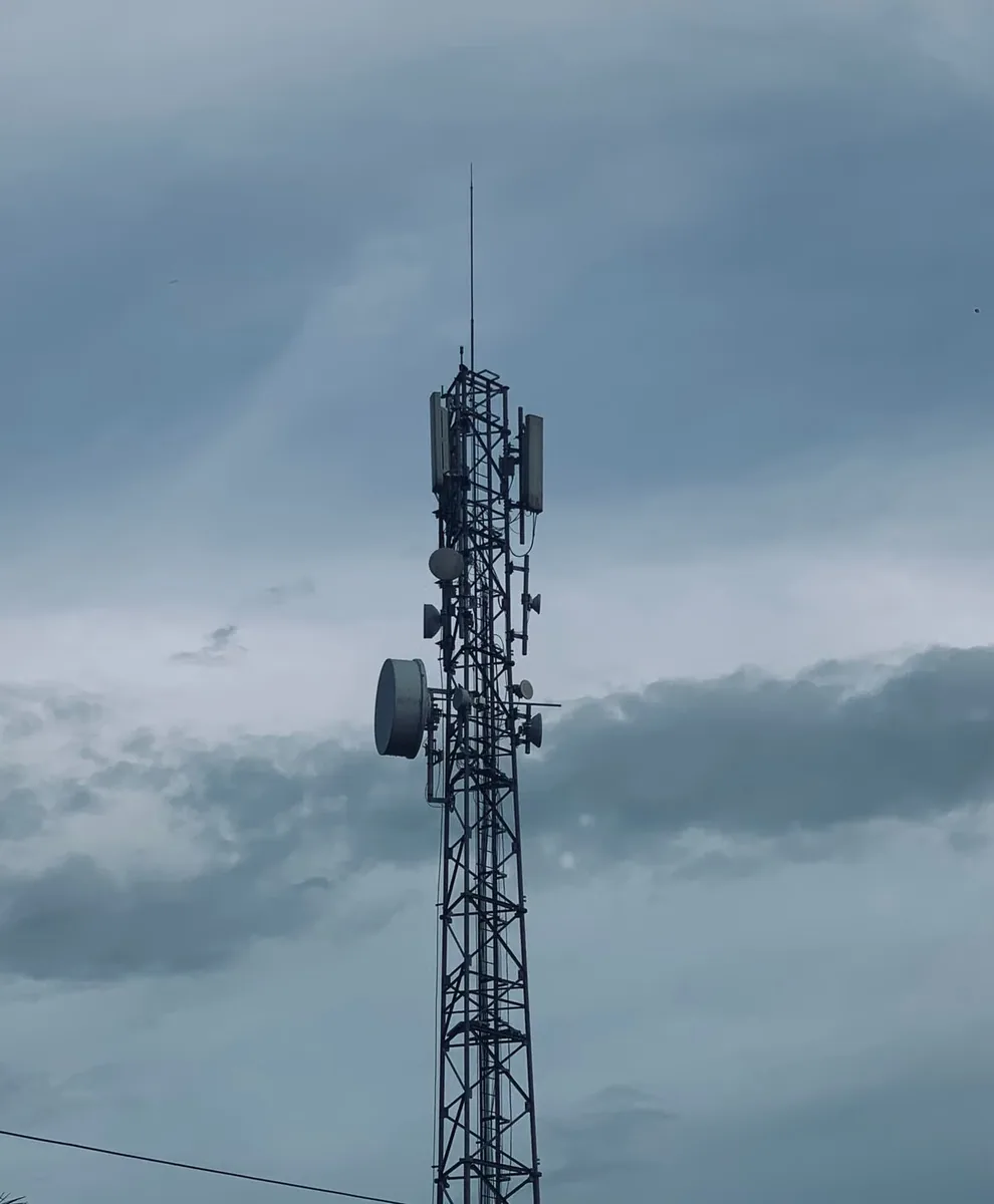
AAU, RRU and RF Power Amplifiers
Transfer concentrated heat into metal chassis. Check local contact area, package load and vertical stability; review thermal and RF behavior together near sensitive circuits.

DU/CU, FPGA, ASIC and Memory
Connect components of different heights to a spreader or housing. Control tolerance, material volume and closure force so contact does not come at the expense of PCB strain.
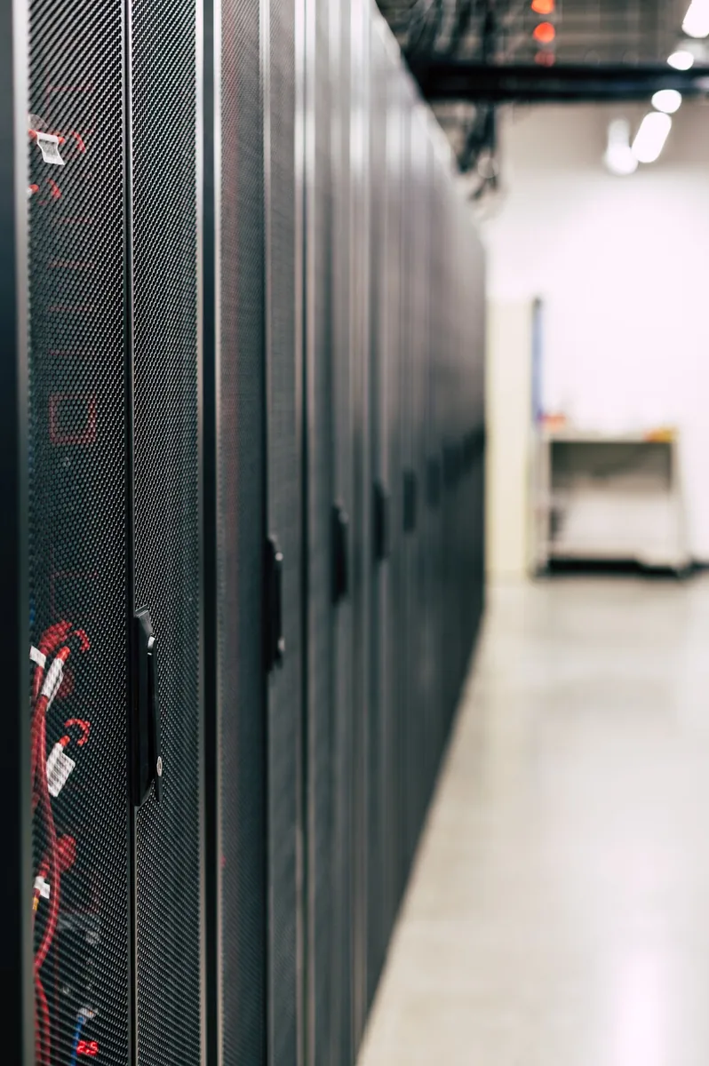
Optical Modules and Network Switches
Define contact to cages, frames or heat sinks under restricted airflow. Validate mating force, insertion and removal, residue and the temperature limit of the selected optical hardware.
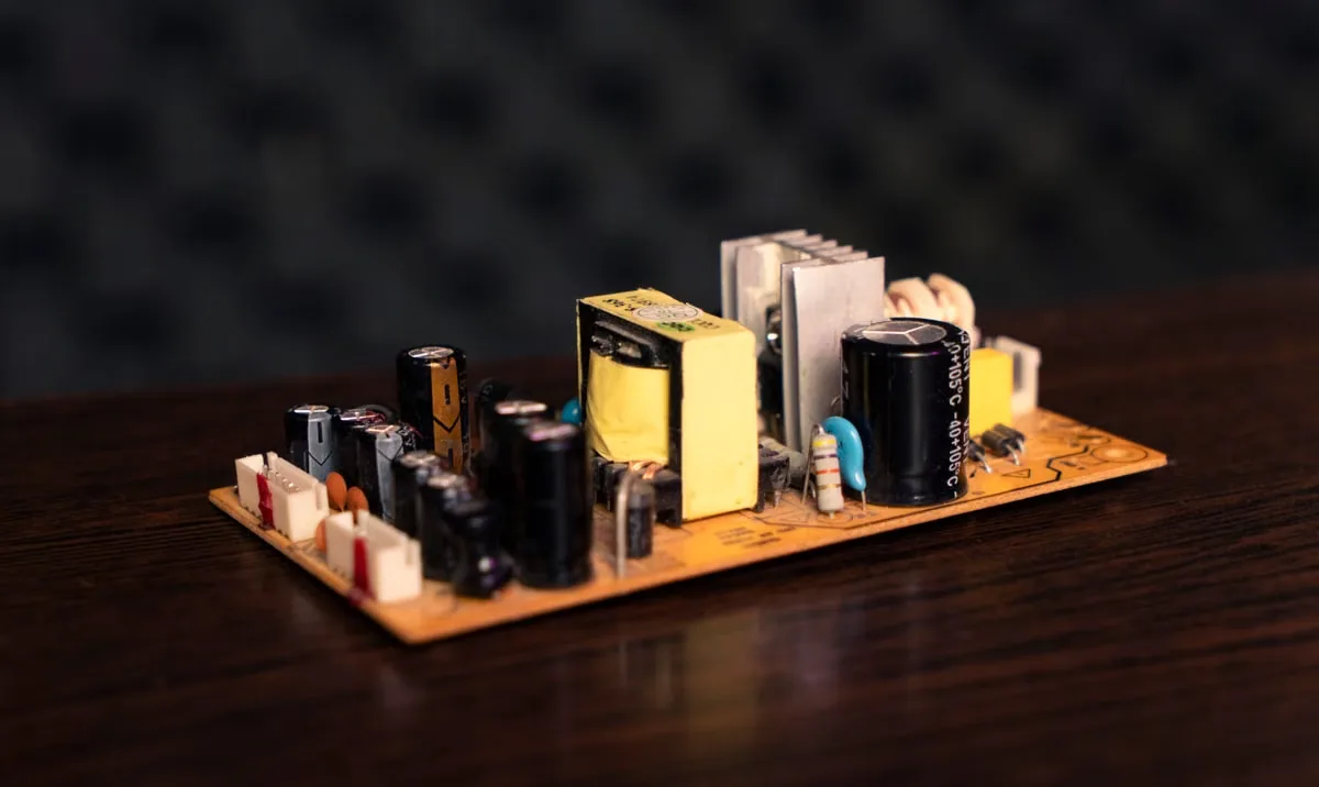
Rectifiers and DC/DC Converters
Move heat from switching devices and power stages into cooling structures. Specify any dielectric requirement at the finished thickness, and inspect contact after electrical and thermal exposure.
Function before formulation
Choosing Thermal Interface Materials for Telecom Equipment
Start with what the interface must do. Then compare grade-specific thermal, mechanical and electrical evidence at the intended assembly conditions.
サーマルパッド
Preformed parts suit repeatable gaps and clean placement. Check compressed thickness, force across the tolerance range, liner release and contact after cycling.
Explore thermal pads →液状ギャップフィラーおよびゲル
Dispensable materials accommodate mixed heights and selective placement. Confirm supplied state, shot volume, open time, shape retention and cure requirements before choosing a production route.
Compare gap fillers and gels →熱伝導グリス
Grease wets surface roughness in thin, mechanically maintained interfaces. It is not a structural gap filler. Qualify dosage, coverage, bleed and pump-out under service cycling.
Review thermal grease →相変化型熱界面材料(TIM)
Preforms or coatings offer controlled initial placement with wetting after activation. Check activation temperature, maintained load, final layer thickness and residue during service removal.
Explore phase change TIMs →Graphite Thermal Sheets
Graphite can spread heat laterally rather than bridge a large gap. Distinguish in-plane from through-plane data; assess conductive edges, isolation layers and the added contact boundaries.
Review graphite thermal sheets →熱伝導性EMI吸収シートパッド
Dual-function materials are candidates where contact and electromagnetic absorption are both needed. Verify response at the relevant frequency, compressed thickness and actual RF layout; absorption is not shielding continuity.
Explore thermal EMI absorber pads →Build a comparable shortlist
Telecom Thermal Material Selection: Gap, Load and Assembly
A usable specification connects material data to the finished hardware. Compare candidates against the same interface and acceptance limits.
| 選択要因 | Define before sampling | 要求する証拠 |
|---|---|---|
| Thermal target | Heat load, component limit, cooler temperature and active area. | Installed temperature or impedance at representative conditions. |
| Gap and bond line | Minimum, nominal and maximum gap; flatness and component heights. | Finished thickness, coverage and contact at tolerance extremes. |
| Assembly load | Fastener sequence, safe pressure and allowable board or package stress. | Force-displacement data and inspection of the actual assembly. |
| Electrical and RF behavior | Voltage, grounding, clearances and any frequency-specific absorption need. | Grade-specific electrical and RF evidence after assembly and aging. |
| Production window | Placement or dispensing method, wait time, cure and line interruptions. | Repeatability, release, shot stability and rework trials. |
| Service exposure | Temperature history, orientation, humidity and mechanical loading. | Post-exposure contact, thermal drift and compatibility inspection. |
Look beyond conductivity
5G Thermal Management Beyond W/m·K
A higher conductivity value does not guarantee a lower component temperature. Thickness, active area and contact at both boundaries affect the installed result.
t = final layer thickness · k = through-plane conductivity · A = effective heat-transfer area. R is in K/W with SI units. This approximation excludes package and cooler spreading resistance; area-normalized impedance has different units.
最終的な厚さ
Use the thinnest complete interface the real gap permits; excess material can lengthen the heat path.
Surface contact
Flatness, finish, wetting and safe pressure determine whether both boundaries remain in contact.
Active area
The part outline may exceed the heat-transfer area. Account for holes, keep-outs and partial contact.
Lifetime stability
Repeat the measurement after exposure. A good initial result is not evidence of sustained contact.
Qualify the finished system
Validate Telecom Thermal Materials for Outdoor Reliability
Establish the initial thermal and electrical result, apply relevant exposure, then retest the same hardware. Test severity should follow the product requirements—not a generic “5G grade” label.
01 / Temperature cycling
Combine self-heating with the intended ambient and solar conditions. Inspect separation, contact loss and thermal drift after representative ramps, dwell and cycles.
02 / Humidity and compatibility
Review coatings, gaskets, contacts and metals near the material. Include condensation, pollutants or salt exposure where relevant; a TIM is not automatically an enclosure seal.
03 / Orientation and vibration
Use the installed vertical or inverted position. Check material movement, fastener relaxation and strain together with the post-exposure thermal result.
04 / Process and service
Repeat placement or dispensing across line starts and stops. Validate removal, cleaning, replacement quantity and remounting if field repair is part of the plan.
From interface brief to sample
Custom Telecom Thermal Materials and Project Review
Share the equipment zone, drawing and acceptance limits. Haktak can review a suitable material family and discuss thickness, cut geometry, packaging or application needs before sampling.
Geometry and load
Gap range, active footprint, fasteners, keep-outs and the maximum allowable assembly force.
Heat and exposure
Heat load, temperature limit, cooling boundary, orientation and lifetime validation requirements.
Assembly and supply
Placement or dispense equipment, cure limits, volume, service plan and preferred delivery format.
For adjacent equipment needs, explore Haktak’s electronic material applications. Review custom die-cutting and converting for preformed interfaces or dispensing process support for liquid materials.
Practical selection answers
Telecom and 5G Thermal Interface Materials FAQ
Which thermal interface materials are used in 5G equipment?
Pads, gels, liquid gap fillers, grease and phase change TIMs connect components to coolers. Graphite sheets spread heat; thermal EMI absorber pads address selected dual-function interfaces. The hardware geometry and required function determine the shortlist.
When should a telecom design use a pad rather than a gel?
A pad is a candidate for repeatable gaps and preformed placement. A gel can suit complex geometry and selective dispensing. Compare force, finished contact, production repeatability and service requirements before choosing either route.
Can thermal grease fill a large component-to-housing gap?
Grease generally serves thin, clamped contacts and microscopic surface irregularities. For a substantial stand-off, evaluate a qualified pad or gap filler at the actual gap range rather than adding a thick grease layer.
What thermal conductivity does a 5G base station need?
There is no universal W/m·K requirement. Start with heat load, temperature limits, cooler boundary, area and final thickness. Compare installed impedance or component temperature under matched conditions and after aging.
How can assembly stress on telecom boards be reduced?
Measure force across the tolerance range and review load distribution, fasteners and material quantity. Select compliance appropriate to the gap while maintaining contact. A hardness value by itself does not establish safe PCB or package loading.
Are all thermal gels stable in vertical radio units?
No. Shape retention depends on the grade, temperature, bead geometry, waiting interval and final assembly. Test slump or migration in the installed orientation, then verify contact after representative service exposure.
Can a thermal pad also reduce RF interference?
Only a material designed and qualified for the relevant electromagnetic function should be used for that purpose. Verify absorption at the actual frequency and compressed thickness. A conventional thermal pad is not automatically an EMI absorber or a conductive shield.
Are telecom thermal interface materials electrically insulating?
Some grades provide insulation; others are electrically conductive. Request evidence for the selected grade at the finished thickness, pressure and exposure conditions. Maintain required clearances and account for conductive edges or squeeze-out.
How should outdoor 5G thermal materials be tested?
Use representative hardware and relevant temperature, humidity, orientation and mechanical exposure. Measure thermal and electrical behavior before and after testing, inspect the interface, and qualify any rework procedure. Enclosure sealing needs separate validation.
What information is needed for custom telecom TIM samples?
Provide the drawing, gap range, contact footprint, load budget, heat load and temperature target. Include electrical or RF needs, assembly equipment, exposure conditions, sample quantity and the acceptance criteria for the trial.