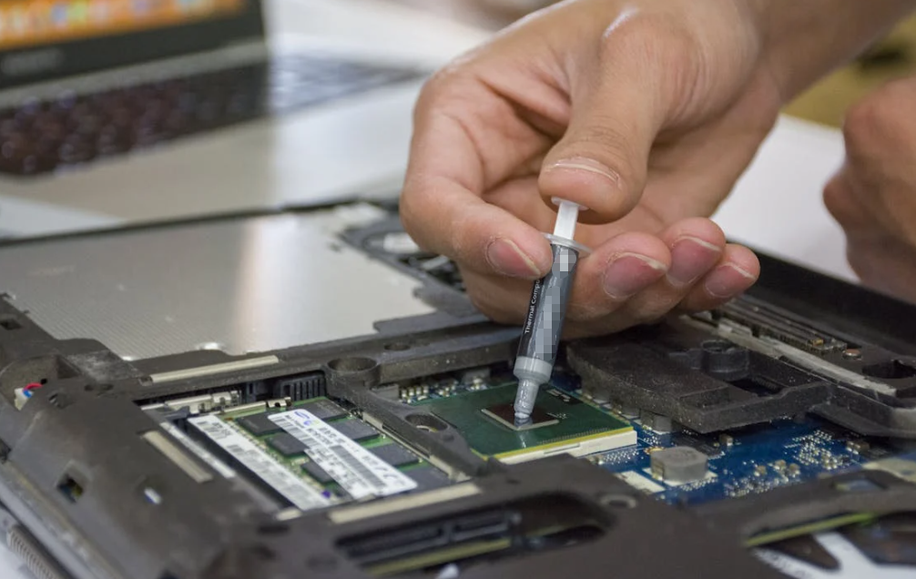
A thermal gap filler is a compliant サーマルインターフェースマテリアル placed between a heat-generating part and a heat sink, cold plate, enclosure, chassis, or spreader.

It replaces air across microscopic surface roughness and larger mechanical gaps caused by component heights, tolerances, board warpage, fasteners, or intentional spacing.
Terminology gets messy. Some suppliers mean pre-formed pads; others mean two-part liquids. Putty and gel may also carry the label. They share a function, not identical processing or mechanics.
Nearby TIMs are not automatic substitutes. Grease suits thin clamped joints, potting fills a volume, and adhesive creates a bond. A gap filler mainly creates a compliant thermal bridge across space.
What Electronic Gap Fillers Are Actually Made Of
Most gap fillers combine a polymer matrix with conductive particles. Think of dough mixed with fine gravel. The matrix controls flow, softness, cure, and aging; the particles carry much of the heat.
The Polymer Matrix Controls Feel, Flow, and Aging
Silicone elastomers are common because they can remain soft across a broad temperature range, accept heavy filler loading, and wet surfaces. Some formulations may release volatile siloxanes or bleed oil, which matters near lenses, relays, contacts, coatings, or later bonding.
Non-silicone materials may use acrylic, polyurethane, or proprietary polymers. They suit defined silicone restrictions, but the label does not promise zero outgassing, zero residue, or perfect compatibility.
The matrix and cure state also affect slump, pump-out resistance, component stress, process control, and rework.
Conductive Fillers Carry Much of the Heat
Fillers include aluminum oxide, boron nitride, zinc oxide, graphite, and proprietary blends. Particle size, shape, treatment, and loading matter. More filler may raise conductivity, but also viscosity, density, hardness, equipment wear, and cost.
Graphite and some metal-filled systems conduct electricity. Many ceramic-filled grades are insulating, but “thermally conductive” alone does not promise dielectric safety.
| Material building block | Why it is used | 主なトレードオフ | 確認事項 |
| Silicone matrix | Softness, stability, wetting | Bleed or siloxane concerns | Volatility, compatibility, aging |
| Non-silicone matrix | Meets silicone restrictions | Chemistry-specific performance and cost | Polymer identity, stability |
| Alumina or zinc oxide | Thermal transfer, possible insulation | Higher density and viscosity | Method, dielectric data, settling |
| 窒化ホウ素 | Heat transfer with insulation potential | Particle design and cost | Through-plane result, hardness |
| Graphite or metal | Heat transfer or spreading | Electrical-conduction risk | Directionality, isolation, edges |
One supplier’s 2026 gap filler selection guide lists pads from 1 to 34 W/m·K. That portfolio range is not an industry rule—or proof that its highest number fits a particular product.

Pads, Putty, Gel, and Liquid Fillers Behave Differently
The material format changes thickness control, assembly force, automation, inspection, and repair. So, start with the joint and factory process—not the name on the bucket.
Pre-Formed Thermal Gap Pads
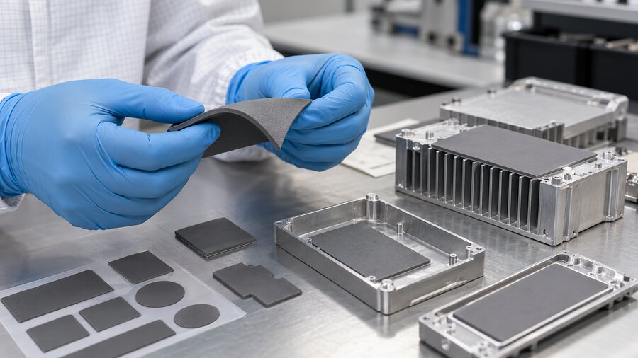
サーマルパッド arrive as sheets, rolls, or die-cut parts. Defined thickness supports clean placement and inspection. Liners, tack, carrier films, and reinforcement aid handling.
Pads suit measurable gaps and repeatable geometry. Too thin may not touch; too thick or firm may bend a PCB, load a BGA, or distort a lid. Very soft grades can stretch or tear during converting.
Moldable or Dispensable Thermal Putty
サーマルパティ conforms to irregular hardware under low pressure and often suits mixed heights or serviceable products.
Control applied mass, position, coverage, vertical stability, residue, and long-term movement. A hand-shaped prototype may hide poor production repeatability. Been there, basically.
One-Part Thermal Gel
A one-part gel is pre-mixed, so it avoids online ratio control and pot life. Some grades remain reworkable; others develop more structure after application.
Check supported gap, storage, settling, dispense pressure, open time, and slump. A small-syringe trial may not predict behavior through a long production hose.
Two-Part Cure-in-Place Gap Filler
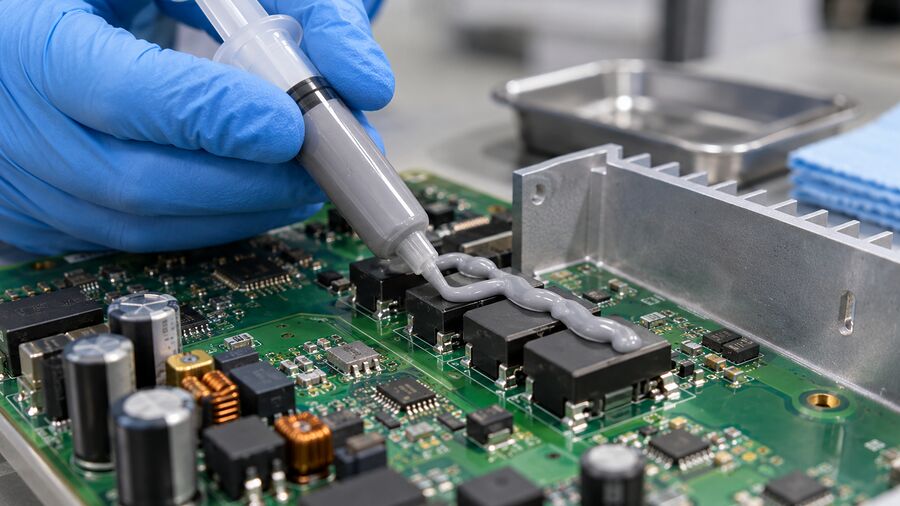
2部構成 液体ギャップフィラー are metered, mixed, dispensed, and cured. They wet complex topography under little assembly force, then form a soft elastomer.
Mix ratio, static mixer, purge, air, pot life, cure temperature, and bead thickness affect the result. Rework is usually slower.
| フォーマット | Best-fit interface | Production advantage | Main watch point | Typical rework |
| Gap filler pad | Defined gap | Clean, visible part | Compression and tolerance | Replace the pad |
| サーマルパティ | Uneven, serviceable joint | Flexible placement | Volume, migration, residue | Often easier |
| 1液型ゲル | Irregular interface | No online mixing | Slump, gap, storage | Grade-dependent |
| Two-part liquid | Complex or large area | Low-stress, cured stability | Mixing, air, cure | More involved |
Choose the Material From the Interface, Not the Label
Start With the Full Gap Range
Measure minimum, nominal, and maximum assembled gaps. Include component tolerance, solder height, PCB bow, housing flatness, coatings, screw sequence, and hard stops. CAD nominal is only the middle of the story.
A useful first-pass relationship for the bulk layer is:
$$R = \frac{t}{kA}$$
Here, $$$$ is thermal resistance, $$$$ is thickness, $$$$ is conductivity, and $$$$ is area. A thicker layer adds bulk resistance. Real results also include contact resistance, voids, spreading, pressure, and wet-out.
だからこそ bond-line thickness affects thermal performance. Aim for the thinnest reliable layer that maintains contact across the tolerance range.
Compare Thermal Impedance Under Relevant Conditions
Bulk conductivity describes material potential. Thermal impedance includes thickness and interface effects. Device temperature shows the system result. They are related, not interchangeable.
Check pressure, thickness, surface finish, temperature, and test method. A soft 5 W/m·K pad may beat a firm 8 W/m·K pad through better contact. Review 熱伝導率と熱インピーダンス before ranking data sheets.
Protect the Electronics From the Interface
Shore 00 hardness helps screen soft pads, but ask for compression-deflection data at the actual thickness and temperature. Also consider modulus, compression set, stress relaxation, area, and lid stiffness.
The interface needs enough force for contact while the PCB stays below its mechanical limit. A balancing act, not a wrestling match.
Add Electrical, Flame, and Cleanliness Requirements
For high-voltage hardware, review dielectric strength, resistivity, puncture, cut edges, creepage, and clearance after compression and aging. Raw-material data is not system approval.
For UL 94, confirm the exact grade, thickness, orientation, and classification. RoHS or REACH paperwork addresses substances; it does not prove cooling or cycling performance.
| Selection variable | Measure or define | Risky shortcut | Better evidence |
| Gap and BLT | Min, nominal, max | CAD nominal only | Production-hardware measurement |
| 熱性能 | Impedance or device temperature | Ranking by W/m·K | Same fixture and conditions |
| 機械的負荷 | Force and component stress | Hardness alone | Assembly deflection measurement |
| 電気安全 | Voltage, edges, spacing | Assuming ceramic means insulating | Grade and assembly tests |
| 清潔さ | Surface and failure mechanism | Unexplained silicone restriction | Compatibility and residue evidence |
| 信頼性 | Cycling, vibration, orientation, life | Fresh coupon only | Before-and-after functional test |

Match Gap Filler Materials to Electronic Applications
Industry frames the risks but does not select the grade. An inverter and camera can both be “automotive electronics” while needing different materials.
| アプリケーション | 一般的なインターフェース | Dominant risk | Useful starting format |
| EV battery and storage | Module to cold plate | Tolerance, vibration, voltage | Soft pad or liquid filler |
| Inverter and power module | Power device to metal | Heat flux, dielectric, cycling | Pad, gel, or cured filler |
| AI server and GPU | Mixed heights to cold plate | Z-height, force, service | Pad, putty, or gel |
| Telecom and outdoor | RF board to enclosure | Slump, cycling, field life | Stable pad or gel |
| LED and industrial | Board to housing | Flatness and hot operation | Pad or dispensed filler |
| Optical, medical, aerospace | Electronics near sensitive surfaces | Contamination and traceability | Qualified clean chemistry |
For aerospace or medical work, “used in the industry” is not qualification. The program, material revision, process, and evidence govern approval.
Material Form Changes the Manufacturing Process

Pads Need Converting and Placement Control
A pad is a complete part. Die-cut geometry, reinforcement, tack, liner, tabs, packaging, and orientation matter. Inspect thickness, damage, contamination, and lot identity; control alignment and closure.
One-Part Materials Need a Stable Dispensing Window
For putty or gel, define temperature, pressure, pump, hose, nozzle, speed, bead, shot mass, and assembly delay. Vision can check position and width, but not always hidden coverage.
Two-Part Materials Add Mixing and Cure Control
Two-part systems need ratio verification, mixer selection, purge, pot-life control, and evidence of cure through the actual volume. A thin lab sample may cure faster than a thick production bead.
Like baking: if the measuring cup lies and the oven runs cold, blaming the flour will not fix dinner.
Common Gap Filler Problems and Practical Fixes
Inspect before disassembly. Opening a lid can smear soft material and erase evidence of movement or contact loss.
| 確認された問題 | 考えられるメカニズム | 最初の管理チェック | Possible correction |
| Hot spot or poor contact | Too little thickness, wrong pattern, warped housing | Map the gap and contact imprint | Adjust volume, thickness, pattern, or hardware flatness |
| PCB bow or package stress | Pad too thick or firm; uncontrolled closure | Measure force and board deflection | Use softer/thinner material or controlled hard stops |
| Internal voids | Trapped air, bead intersection, fast closure | Section or image a representative interface | Change bead path, purge, nozzle position, or closure speed |
| Squeeze-out into keep-outs | Excess volume or weak hot stability | Weigh shot and inspect after hot dwell | Reduce volume or add escape and keep-out space |
| Slump or pump-out | Rheology, gravity, thermal movement, vibration | Compare orientations before and after cycling | Select a more stable grade or revise retention and gap |
| Oil bleed or residue | Chemistry or aging mismatch | Identify residue and affected function | Use a qualified low-bleed or alternative chemistry |
| Soft or uncured regions | Ratio, mixing, time, or temperature error | Check dispense records and cure through volume | Correct metering, mixer, purge, and cure profile |
| Cracking or delamination | High cured modulus, weak surface contact, CTE strain | Locate cohesive versus interface failure | Change modulus, surface preparation, or joint mechanics |
Change one major variable at a time. Switching material, torque, bead, and cure together teaches almost nothing.

Standards Help You Test; They Do Not Choose the Material
ASTM D5470-17(2024) covers steady-state thermal impedance and apparent thermal conductivity for thermally conductive electrical insulation materials. ASTM includes viscous liquids, viscoelastic solids, and rigid solids in its material types. It also warns that its idealized, uniform heat flow cannot be applied directly to most practical assemblies.
Other useful references depend on the question:
- ASTM D149 may support dielectric-strength testing of suitable solid or cured insulating specimens.
- ASTM D575 addresses compression-deflection behavior of rubber materials when its specimen and method fit the construction.
- UL 94 covers small-scale flammability classifications for polymer specimens.
- ASTM E595 is relevant to outgassing screening for applicable vacuum or spacecraft materials.
- IEC 60068-2-14:2023 provides change-of-temperature tests.
- IEC 60068-2-64 covers broadband random vibration.
- ISO 16750-3 and ISO 16750-4 may support mechanical and climatic programs for road-vehicle electronics.
The customer specification and product risk decide which methods apply. A UL classification does not predict thermal impedance. A D5470 result does not prove vibration life. A useful plan combines 一般的なTIM試験規格 with assembly-level temperature, mechanical, electrical, and aging tests.

Build a Useful Supplier Brief Before Requesting Samples
Send more than “Need 8 W/m·K gap filler.” Include:
- Interface drawing, contact area, substrates, and cooling surface
- Minimum, nominal, and maximum assembled gap
- Heat load, heat flux, temperature target, and operating range
- Available pressure, component force limit, and closure method
- Voltage, dielectric, flame, contamination, and chemical requirements
- Pad placement or dispensing equipment and target cycle time
- Orientation, thermal cycling, vibration, humidity, and expected life
- Rework plan, sample quantity, annual volume, and acceptance criteria
That information makes 材料選定と試験 much faster. More importantly, it helps the supplier recommend a material-process pair instead of guessing from one attractive number.
結論
The best gap filler material is not automatically the softest pad, the most stable cured gel, or the product with the highest conductivity. It is the option that fills the real interface, keeps component stress acceptable, supports the manufacturing process, and maintains thermal and electrical performance after aging.
Start with gap, pressure, geometry, and risk. Narrow the material family next. Compare individual grades only after that. A little less glamorous than shopping by W/m·K, sure—but far more likely to survive production.
よくある質問
What is a gap filler material in electronics?
A compliant TIM placed between a heat source and heat sink, cold plate, enclosure, or chassis. It replaces air, conforms to uneven surfaces, and transfers heat across the gap.
What are thermal gap fillers made of?
Most combine a silicone or non-silicone polymer matrix with alumina, boron nitride, zinc oxide, graphite, or proprietary particles. Composition controls thermal, mechanical, electrical, and processing behavior.
What is the difference between a thermal pad and a liquid gap filler?
A pad is pre-formed with defined thickness. A liquid is dispensed across complex surfaces or variable gaps. Pads simplify placement; liquids reduce assembly force but require dispense and sometimes cure control.
Is a silicone or silicone-free gap filler better?
Neither is universally better. Silicone offers broad softness and temperature capability. Silicone-free systems address defined restrictions. Compare thermal performance, contamination evidence, reliability, process, and cost in the assembly.
Is higher thermal conductivity always better for a gap filler?
No. Bond-line thickness, contact resistance, pressure, coverage, and aging also matter. A lower-conductivity material may perform better when it creates thinner, more complete contact.
How thick should an electronic gap filler be?
It must fill the maximum assembled gap without creating excess resistance or force at the minimum gap. Validate the compressed or cured bond line on production-intent hardware.
How much should a thermal gap pad be compressed?
Use force-deflection data for the exact grade and thickness. There is no universal percentage. Maintain contact without exceeding limits for the PCB, packages, solder joints, or housing.
Are thermal gap fillers electrically insulating?
Many ceramic-filled products insulate, but graphite- or metal-filled materials may conduct electricity. Confirm grade-specific dielectric strength, resistivity, thickness, edge condition, and system-level performance.
Can thermal paste replace a thermal gap pad?
Usually not across a large gap. Paste suits thin, flat, clamped interfaces and may pump out when too thick. Putty or liquid filler often fits uneven gaps better, subject to testing.
How should gap filler reliability be tested?
Test the installed interface at realistic gap, pressure, surfaces, orientation, and power. Retest after relevant aging, cycling, humidity, vibration, or shock. Inspect migration, voids, cracks, bleed, cure, and clamp condition.