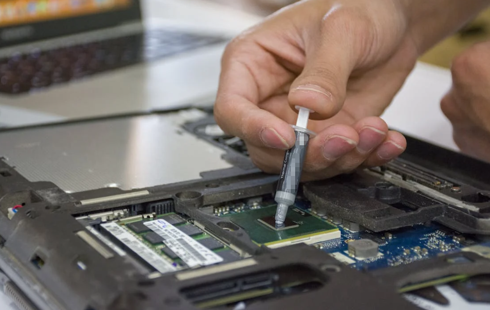
Pick up a fresh copper-clad board and it looks a bit like a road map before anyone has drawn the roads. Copper covers the surface. Your circuit only needs some of it: the narrow paths between components, the places where parts will attach, and perhaps larger areas for power or ground. The rest has to go.
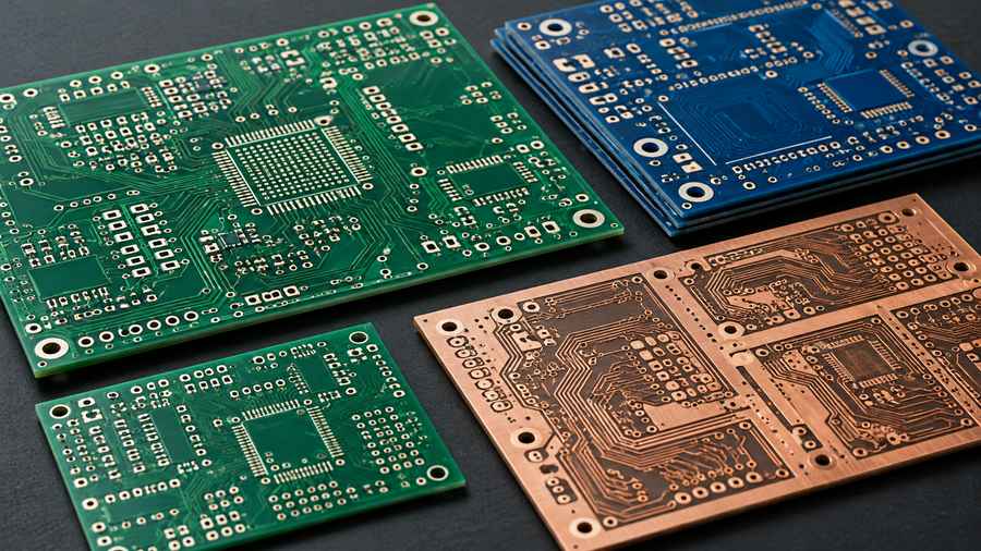
PCB etching is one way to remove that unwanted copper. First you protect the pattern you want to keep. Then an etching process takes away exposed copper. Peel back the protection, and the electrical layout appears.
Simple enough as an idea. Choosing the best way to do it is trickier. A student making one roomy circuit has different needs from a factory making thousands of boards with tiny traces. And “etching solution” might mean a bottle of liquid or the whole approach to making the board. Let’s sort out both.
What Does PCB Etching Actually Remove?
Most familiar printed circuit boards start with a sheet of insulating material bonded to copper foil. FR-4 glass-epoxy laminate is a common rigid-board base, though flexible and metal-backed boards use different constructions. Etching removes selected areas of the Messing, leaving the pattern specified by the design.
The remaining copper may form traces, which connect points across the board; Pads, where a component or test probe can touch the circuit; and broader planes for power, ground or other functions. The insulating material keeps separate copper paths from making accidental contact.
Here is the small mental picture that helps: lay a stencil over a copper sheet. The stencil covers the paths you want. An etchant reaches the uncovered copper and removes it. In PCB work, the stencil is usually called an etch resist. It might be a patterned photoresist in a factory or another suitable mask in a simple prototype process.
This is a subtractive process. It starts with more copper than the circuit needs and takes material away. There are other ways to build conductive features, but they are separate manufacturing routes. Also, an etched board is still a bare PCB. Drilling, plating, surface finish, inspection and component assembly may all be needed before it becomes a working electronic product.
One more thing: the coating that protects copper during etching is not automatically the green solder mask you see on a finished board. They serve different stages of the build.
How Does the PCB Etching Process Work?
The exact factory sequence depends on whether a layer is inside a multilayer board, on the outside, or part of a different fabrication flow. Still, the basic logic is steady: define the image, protect the copper to keep, remove exposed copper, and check the result.
1. Design the copper pattern
An engineer starts with a schematic and PCB layout. The layout defines trace paths, pad shapes, spacing, copper areas and connections between layers. Before fabrication, the team should check whether the selected board shop can actually make the requested features on the specified copper thickness.
Think of drawing a narrow road on paper. If the printing process tends to nibble away a little from each side, the final road might be narrower than the line you drew. Board designers and fabricators work together on those allowances. A screen image alone is not a promise of the final conductor width.
2. Apply and pattern the resist
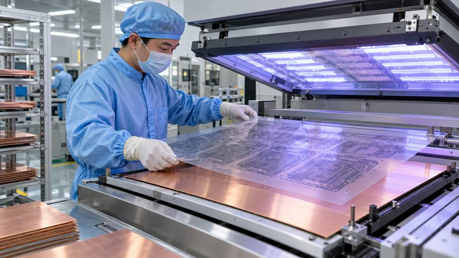
Copper needs a protective pattern before the main etch. In a photofabrication flow, photoresist is applied to prepared copper, exposed through artwork or imaged directly, and developed. Which areas stay protected depends on the particular resist and image process. You cannot assume that every exposed area behaves the same way across different systems.
For a simple educational board, a toner-transfer mask is another known approach. It can demonstrate the principle, but gaps, poor adhesion and rough edges become frustrating when the traces get fine. Factories use controlled imaging, material preparation and inspection because a missing bit of resist can become a missing bit of trace.
3. Remove the exposed copper
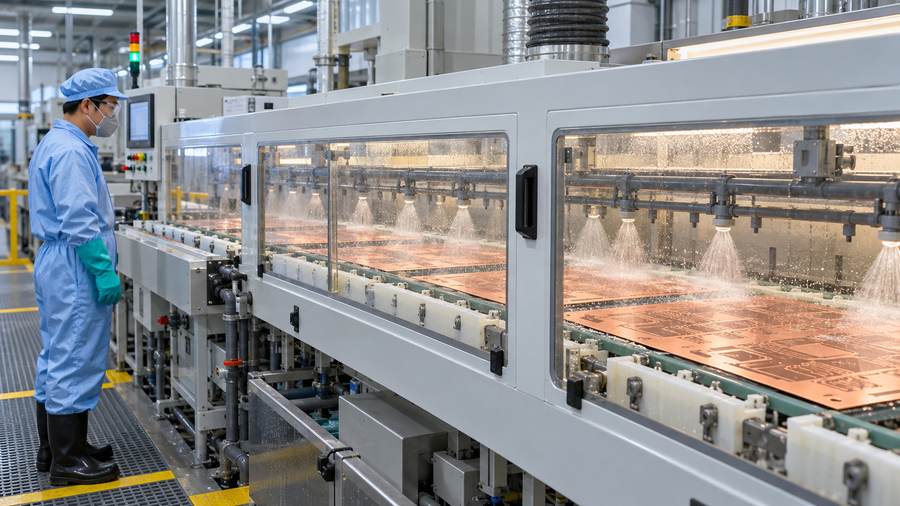
The prepared board reaches the etching stage. In wet chemical etching, the process liquid reacts with accessible copper while the masked pattern remains. Industrial lines may use controlled spray application; a basic prototype may use a different, smaller-scale method. Bath condition, flow, temperature, copper loading and exposure all affect the result.
People in fabrication often talk about a develop–etch–strip, or DES, sequence. Developing reveals the intended copper to remove. Etching removes it. Stripping takes off the remaining process resist. Outer-layer production may use a metallic etch resist and plating steps that differ from an inner-layer photoresist flow. It is better to ask how a specific shop builds your board than to assume one generic diagram describes every stack.
4. Clean, inspect and continue the board build
After etching, the manufacturer checks for unwanted copper bridges, open or thin traces, rough edges and other defects. A multilayer board still needs the right layer alignment, lamination and interlayer connections. Depending on the fabrication route, holes, plated vias, solder mask, exposed-pad finish, electrical testing and other checks follow or occur elsewhere in the sequence.
Finally, an assembler mounts and solders components. That is when the patterned copper starts doing its intended job as part of an actual circuit. The distinction sounds picky, but it prevents a lot of confusion when someone says a board is “finished.” Finished at which stage?
Which PCB Etching Liquid Fits Which Job?
There is no bottle that wins every comparison. Etchant choice depends on the protective mask, the copper being processed, the equipment, required feature quality, throughput, chemical management and an approved route for spent solution. Even two boards with the same outline can require different process choices.
| Etchant family | Where it may fit | Main trade-off to check |
|---|---|---|
| Ferric chloride | Common commercially supplied option for straightforward copper etching and educational prototyping | Staining, handling, bath condition and copper-bearing waste; follow the exact product documentation |
| Ammonium persulfate | Another commercially supplied copper etchant for small-scale processes | Oxidizer handling and changing bath performance; “clearer” does not mean harmless |
| Cupric chloride system | Controlled professional copper-etching lines, including processes designed around bath regeneration | Needs suitable equipment and close chemical/process control |
| Alkaline ammoniacal system | Certain production processes, often matched to specific outer-layer masking or metallic resist | Mask compatibility, ventilation and tightly controlled plant operations |
For a first learning board, a product sold specifically for PCB etching is easier to evaluate than a homemade mixture with an uncertain composition. MG Chemicals’ copper etchant range shows that even a single prototyping supplier offers more than one chemistry. The package, technical data and safety data sheet for the exact product matter more than a generic online claim that one chemical is always faster or cleaner.
In a factory, copper-chloride and alkaline systems are part of a complete line. A bath can be controlled, replenished or regenerated under the plant’s operating method. You would not choose that system by its name alone. You would compare the needed copper geometry, mask, spray equipment, throughput and waste treatment.
Please do not treat a “less messy” appearance as an environmental verdict. The liquid after etching contains dissolved copper. What happens to that copper is part of the process cost and the responsibility of whoever runs it.
Chemical Etching, Milling or Laser: What Is the Better Route?
If the real question is “How do I make this circuit pattern?”, chemical etching is not the only option. But the alternatives are not interchangeable, either.
Wet chemical etching removes unprotected copper through a controlled reaction. Once the imaging and process are set up, it can reproduce a pattern across panels and production runs. The mask, chemistry and process control are inseparable parts of that result.
Isolation milling uses a rotating tool to cut copper away around desired traces. There is no copper etchant bath. For certain simple, immediate prototypes, it can be convenient. The trade-offs include tool wear, surface flatness, burrs and dust. Milling around copper islands also does not, by itself, give you plated through-holes, a multilayer stack or a production-ready solder mask.
Laser methods need more precise wording. A laser can mark a board, remove a resist or coating, or directly remove some copper with suitable equipment. Those are three different jobs. Seeing a product advertised as a “PCB laser” does not prove it can produce your copper width, substrate quality and repeatability. Plasma processing is another specialized tool; it is not automatically the standard replacement for a production wet-etch line.
| Project | Likely starting route | Warum |
|---|---|---|
| A spacious, single-sided learning circuit | A documented small-scale etching setup or suitable isolation milling | Demonstrates the patterning principle without pretending to be a production build |
| A one-off layout check today | In-house milling or another controlled prototyping route, if the necessary tools are available | Fast feedback on a simple layout; inspect actual trace quality |
| A repeatable two-layer product board | Qualified PCB fabricator | Controlled imaging, drilling, plating, mask, inspection and records matter beyond the etch |
| Fine-pitch, HDI or multilayer board | Fabricator with demonstrated capability for the whole construction | Layer registration, vias, line geometry and testing cannot be solved by choosing a liquid |
The “best” route changes with what the prototype is meant to prove. A hand-etched board can teach circuit behavior. It may be a poor stand-in for validating fine-pitch soldering or the reliability of a production stack. That difference is easy to miss when a quick bench result looks tidy.
What Controls Trace Accuracy During PCB Etching?
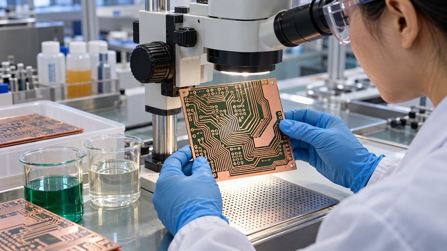
The etched line is the outcome of several steps, not just the time spent in an etching machine. Start with the copper thickness and feature size. More copper has to be removed from a thicker foil, while a very narrow intended trace leaves less room for side loss. A mask with fuzzy edges gives the chemistry a fuzzy boundary to work against.
Then there is undercut. The etchant attacks downward through the exposed copper, but it can also eat sideways beneath the edge of the resist. Imagine cutting a cookie with a cutter that nibbles a little under the dough you hoped to keep. The top image and the final copper edge do not match perfectly. The fabricator may compensate in the artwork and control the process so the finished width meets the agreed requirement.
Flow matters too. On a large panel, one area may receive fresh etchant differently from another. Spray condition, nozzle maintenance, etchant strength, dissolved copper, temperature and conveyor dwell all influence removal. The resist must stay attached throughout the run. If it lifts locally, copper you meant to keep may disappear.
The design also affects the result. Closely packed thin traces beside large exposed areas can be harder to process uniformly than a roomy board. Copper balance and feature distribution are subjects for a design-for-manufacture review, not reasons to invent a single safe trace width for every shop.
An engineer should ask the fabricator a practical question: What finished line and space can you deliver on this copper construction, at the quality level we need? Share the stack-up, copper requirements and quantity. Compare the answer with the finished-board inspection plan. If someone offers one universal tolerance without knowing the process, take a breath and ask for the conditions.
Common PCB Etching Defects and Where to Look First
When a board comes out wrong, changing the chemical is tempting. Sometimes that is relevant. Often the problem began before the board reached the etch stage, or sits in an uneven process condition.
| Was Sie sehen | First checks | Reasonable response |
|---|---|---|
| Copper remains where isolation was expected | Image development, exposed-copper coverage, process liquid condition and flow | Restore the intended image and process window; inspect more than one panel area |
| Traces are thinner than specified | Artwork allowance, copper thickness, dwell and undercut | Review finished dimensions with the fabricator; adjust imaging or process controls |
| Jagged edges or missing pieces | Resist cleanliness, adhesion and image quality | Fix the mask or preparation step before increasing etch strength |
| A copper bridge shorts neighboring paths | Image defect, insufficient copper removal or inspection escape | Locate the bridge and correct the relevant imaging or etch condition |
| Results vary across the panel | Spray/flow pattern, temperature, chemistry and panel layout | Map the variation, then change and verify one control at a time |
For example, imagine a little power-supply board with a fat ground area and several narrow control traces. The center looks fine, but narrow paths along one edge come out ragged. It is tempting to leave the next panel in longer. That could remove the stubborn copper and also over-etch the good traces. First compare the image quality and flow across the panel. Fix the cause, not merely the clock.
Inspection is part of the answer. Check the pattern against the agreed drawing and acceptance criteria, then use suitable electrical checks. A pretty photo does not tell you whether an almost invisible bridge or open remains.
Where Does Etching Matter Across Industries?
The copper-removal principle stays similar; the consequences of a bad pattern change with the product. An industrial controller may carry power and low-voltage signals on the same board. A telecom unit can be sensitive to the geometry of fast signal paths. An EV control board may have to survive cycling and vibration. Compact consumer hardware pushes routing into tight spaces. LED products bring heat-path questions alongside the circuit design.
The substrate choice belongs in that wider picture. FR-4 serves many general-purpose rigid boards. Polyimide can support flexible constructions. A metal-core LED board may help spread heat. These materials are not simply different brands of etching liquid; they shape the full board build and what the fabricator can reliably process.
For a practical LED example, trace layout carries power to the emitters, while the finished module still needs a way to move heat toward its housing. HAKTAK’s LED lighting thermal-material overview deals with that later heat path. A better etch pattern cannot fill a mechanical air gap under the assembled board.
Safety, Copper Waste and Board Quality Standards
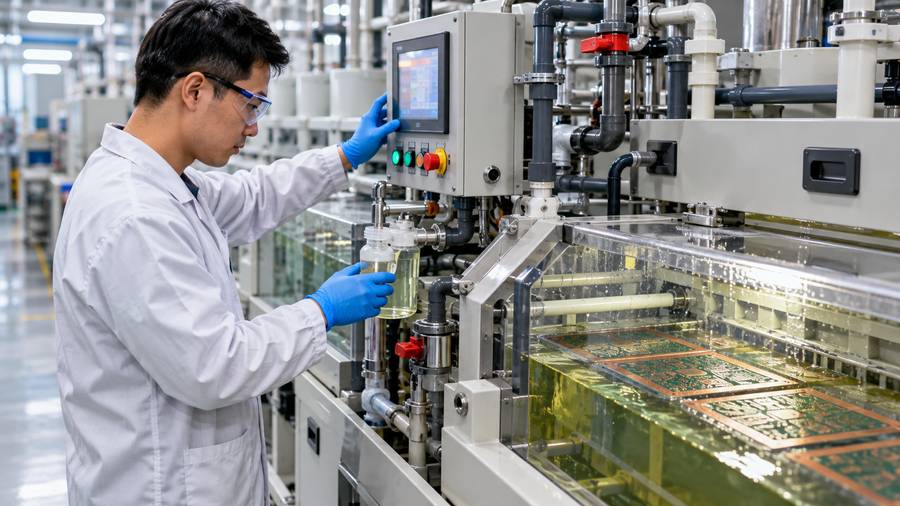
Etchants are process chemicals, not craft-store colored water. Use the instructions and safety data for the selected product, suitable training, containment and protective equipment. The work area and any disposal arrangement must fit the local rules and the quantity being handled. This article is a selection guide, not a substitute for a process sheet.
Spent solution contains dissolved copper. A neutral-looking pH does not remove that metal. Keep the liquid out of drains and ground unless the applicable authority and approved treatment route explicitly allow a particular discharge. A facility may use recovery or a permitted waste service. The US EPA guide to PCB-manufacturing waste streams explains why copper-bearing process waste needs its own plan; use current local requirements to decide what applies today.
Standards are another place to avoid mixing stages. The IPC-2220 family helps frame board design. IPC-6012 covers qualification and performance requirements for rigid bare boards. IPC-A-600 describes observable bare-board acceptability conditions. The IPC standards overview helps distinguish their roles. Which revision, class and acceptance criteria apply should be agreed with the fabricator. These standards do not mean that one named etchant is automatically approved for every board.
After Etching: From Bare Copper to a Protected Assembly
An etched image is a milestone, not the finish line. The board still needs whichever layer bonding, holes, plating, solder mask, surface finish and tests its construction calls for. Then components are mounted and soldered. Only now can the product team judge how the circuit, enclosure and operating environment behave together.
The questions change at this point. Will condensation reach the assembled board? Is a heavy component supported? Does a power device have a sound route to the housing? HAKTAK’s semiconductor and electronics assembly materials distinguish coating, underfill, potting, bonding and thermal interfaces according to their different jobs. A PCB-compatible electronic adhesive may support a particular bond or assembly operation, but its cure and material compatibility still need checking.
If a metal cover sits above components of several heights, the assembled board may also need a compliant thermal interface. The guide to thermal putty for uneven component heights shows how board bow and closure force affect that choice. None of those products etches copper. They address the next problems the finished electronics face.
So What Is the Best PCB Etching Solution for Your Project?
Write down what “best” must mean before naming a chemical or machine:
- What finished trace and gap dimensions are required, on what copper thickness?
- Is this a teaching exercise, a functional prototype or a production-qualified board?
- Does the construction need plated vias, multiple layers, controlled geometry or a special laminate?
- How many identical boards are needed, and when?
- Who will inspect them and manage the chemical or machining waste?
For a simple experiment, a documented commercial etchant process or suitable milling setup may answer the question. For a dense or repeatable product, ask a PCB fabricator to demonstrate the whole build capability. You are buying a finished, testable board, not merely a faster way to dissolve copper.
Fazit
PCB etching protects the copper a circuit needs and removes the rest. The idea is easy to picture. Getting accurate, repeatable traces takes a good image, a compatible process and a way to check the finished board.
There is no single best liquid for everyone. A bench prototype, a factory panel and a fine-feature multilayer board ask different things of the process. Choose from the board’s real requirements, plan for copper-bearing waste, and remember that the etched pattern is only one step toward reliable electronics.
Häufig gestellte Fragen
What does PCB etching do?
It removes selected copper from a copper-clad board so the intended traces, pads and other conductive features remain. A patterned resist usually protects the copper the design needs.
Which chemical is used to etch a PCB?
Common examples include ferric chloride and ammonium persulfate for some prototyping setups. Controlled factory processes may use cupric-chloride or alkaline chemistry. The right choice depends on mask compatibility, board requirements, equipment and waste controls.
Is ferric chloride better than ammonium persulfate?
Neither is best in every situation. Compare the exact commercial products’ instructions, the quality needed, the equipment available and how spent copper solution will be handled. A clearer-looking liquid is not automatically safer.
What is photoresist, and why is it used?
Photoresist is a light-patterned material used to protect selected copper during fabrication. It helps transfer the circuit image onto the board. If its pattern has gaps or lifts, the finished copper can have missing or damaged features.
What causes undercut or thin PCB traces?
Wet etching can remove copper sideways beneath a resist edge as well as downward through exposed copper. Mask quality, copper thickness, flow and process time all matter. The fabricator should verify finished dimensions against the agreed design.
How long does PCB etching take?
There is no useful universal time. Chemistry, copper thickness, equipment and the specific process window affect the etch stage. Imaging, cleaning, inspection and the rest of fabrication add time beyond that stage.
Can I etch a PCB at home?
A simple educational board may be possible with suitable training, product instructions, protective measures and an approved plan for spent solution. Fine-pitch, plated-through-hole or multilayer work calls for a capable fabrication process. Do not use an improvised chemical recipe as a shortcut.
Why did my resist or toner pattern fail?
Possible causes include dirty copper, poor transfer or exposure, damaged artwork and weak adhesion. Inspect the image before etching. If the pattern has a broken line then, leaving the board in the etchant longer will not put it back.
Is PCB milling the same as etching?
No. Milling uses a cutting tool to remove copper around desired paths. Chemical etching uses a process liquid and protective mask. Both can define a circuit pattern, but their equipment, limits and waste streams differ.
Can used etchant go down the drain after neutralizing it?
Do not assume so. Neutralizing acidity does not remove dissolved copper. Keep spent liquid contained and use a disposal or recovery route accepted under the rules that apply where the work is done.