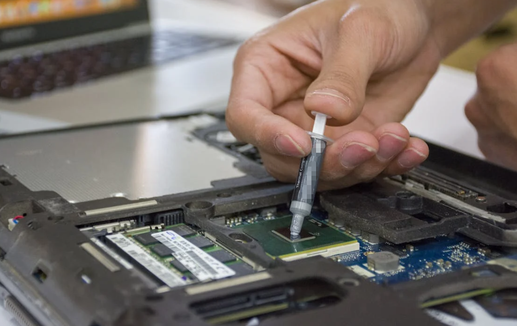
Thermal pads move heat from telecom components into a heat sink, chassis or cast-metal enclosure while filling the real gaps left by component height, PCB bow and housing tolerances. In 5G base stations, they are commonly used around RF power amplifiers, FPGAs, power supplies and control electronics. The right pad must transfer heat et compress safely, insulate where required and survive the outdoor service environment.

That sounds simple enough. Put something soft between the hot part and the cold metal, tighten the enclosure, job done. In practice, this interface is where thermal, mechanical and electrical decisions collide. A pad with an impressive conductivity number can still perform badly if it is too thick, too hard or only touches half the intended surface.
This guide explains how thermal pads work in active antenna units, remote radio units, baseband equipment, telecom routers, switches and edge systems. It also covers material options, test methods, common mistakes and the information a supplier needs to recommend a practical part.
Planning a telecom thermal stack-up?Contact Haktak’s material team with the component drawing, gap range, operating temperature and insulation requirement. You can also review Haktak’s broader thermal interface material portfolio.
Why Thermal Management Is Harder in 5G Telecom Equipment
5G equipment places high-power RF electronics, digital processing and power conversion into compact packages that may operate continuously in sealed outdoor housings. Heat must cross several imperfect interfaces before it reaches the enclosure and ambient air. More integration shortens electrical paths, but it also concentrates heat and leaves less room for fans, large heat sinks or generous mechanical clearances.
An active antenna unit, or AAU, combines antenna elements with radio functions that older architectures often kept separate. A remote radio unit, or RRU, may contain power amplifiers, filters, transceivers, FPGAs, DC-DC converters and control boards inside a weather-resistant aluminum enclosure. Small cells and edge gateways create the same problem on a smaller scale: plenty of processing, not much free air.
The thermal challenge is rarely one hot chip. It is a chain:
- Heat leaves the semiconductor junction and package.
- It crosses solder, substrate or package attach layers.
- It moves through a thermal pad or another interface material.
- It spreads into a cold plate, heat sink or enclosure wall.
- It finally reaches outdoor air by natural convection and radiation, or by forced air in indoor equipment.
Every link adds thermal resistance. A weak interface can raise component case temperature even when the external heat sink looks substantial.
Outdoor installations add another twist. The enclosure may see direct sun, cold starts, wind, humidity, condensation, dust, salt-laden air or rapid load changes. The electronics heat up from the inside while the weather pushes from the outside. It is a bit like trying to keep a kitchen oven stable while someone keeps opening the window.
Le ETSI Environmental Engineering committee classifies environmental conditions for telecom equipment in locations such as telecom centers, street cabinets, pole-mounted equipment and non-weather-protected sites. Those classes are useful when the complete equipment test plan is built. They do not, by themselves, prove that one pad is suitable. The material still has to be validated in the actual assembly.
Where Thermal Pads Are Used in 5G Base Stations
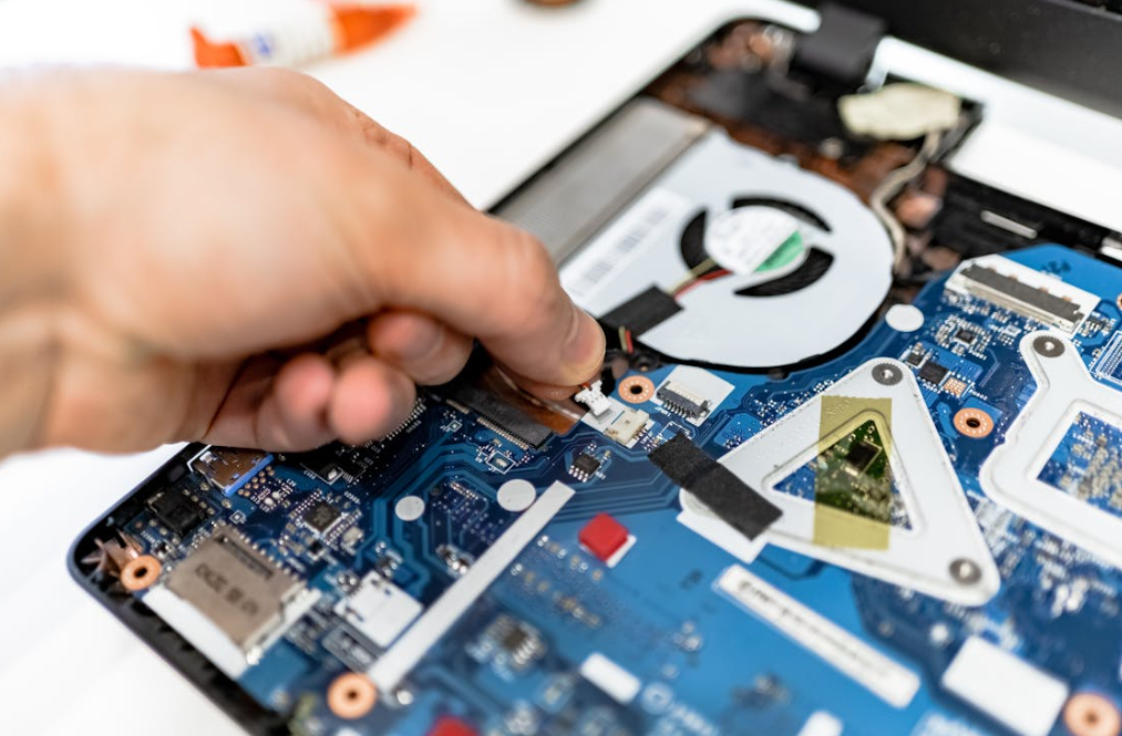
Thermal pads are most useful where a heat-generating component must couple to a cooling surface across a measurable or variable gap. Their softness lets them conform to surface roughness and part-height variation. In telecom equipment, the cooling surface is often the inside wall of a die-cast aluminum enclosure, a machined heat spreader, an EMI shield or a dedicated heat sink.
RF Power Amplifiers and Front-End Modules
The RF power amplifier is a major heat source in many radio units. Its electrical efficiency is not 100 percent, so some input power becomes heat near the antenna path. A pad may bridge the amplifier package, local spreader or PCB region to the radio housing. The design must control bond-line thickness and pressure without bending the board or overloading solder joints.
For a power amplifier, low installed thermal impedance often matters more than the largest W/mK value printed on a datasheet. A slightly lower-conductivity pad that compresses into a thin, complete contact layer can outperform a hard, high-conductivity pad that bridges only the tallest points.
FPGAs, ASICs and Baseband Processors
FPGAs and application-specific processors handle beamforming, coding, packet processing and control tasks. Their packages can sit at different heights from neighboring memory and power devices. A custom die-cut pad can cool one device or cover a group, provided the compression pattern has been checked.
Large packages deserve extra care. Too much force can bow the PCB, stress balls under a BGA package or distort the enclosure. When the gap varies widely across the board, using one very hard sheet over everything is usually not a clever shortcut.
DC-DC Converters and Power Modules
Power supplies generate heat in switching devices, magnetics, rectifiers and control ICs. Electrically insulating thermal pads can transfer that heat to a metal chassis while helping maintain the required voltage isolation. The electrical requirement should be stated as a system need, not guessed from pad thickness alone.
Filters, RF Shields and Supporting Electronics
Not every interface is chip-to-heat-sink. Pads may couple metal shields, filter housings, controller boards or localized spreaders to the main enclosure. These locations may run cooler than the power amplifier but have larger gaps or more uneven surfaces.
Routers, Switches, Optical Transport and Edge Equipment
Telecom thermal pads are also used in indoor network equipment, optical modules, industrial gateways, customer-premises equipment and outdoor 5G routers. The heat path may connect processors, PHY devices, optical transceivers, power-over-Ethernet circuits or SSDs to a chassis. Airflow is more common indoors, but good conduction still prevents local hot spots and fan speed from climbing unnecessarily.
| Equipment or component | Typical cooling interface | What the bloc-notes must handle |
| AAU or RRU power amplifier | Package or spreader to cast housing | High local heat flux, flatness variation and controlled pressure |
| FPGA, ASIC or baseband processor | Package top to lid or heat sink | Package protection, gap tolerance and stable impedance |
| DC-DC converter or power module | Device or PCB area to chassis | Heat transfer plus dielectric isolation where required |
| RF shield or filter | Metal can to enclosure | Larger contact area, tolerance variation and vibration |
| Telecom router or switch | Processor, PHY or power circuit to chassis | Long service life, cycling and possible forced-air assistance |
| Outdoor gateway or CPE | SoC and modem to sealed housing | Passive cooling, weather exposure and compact assembly |
| Optical transport equipment | Transceiver region or control IC to spreader | Local hot-spot control and clean die-cut geometry |
What Is a Thermal Pad, Exactly?
A thermal pad is a compliant, solid-form thermal interface material designed to replace insulating air at a mechanical joint. It is supplied as sheets, rolls or die-cut parts and is normally compressed during assembly. Unlike thermal grease, it does not flow freely. Unlike structural adhesive, it is usually intended to remain removable and does not carry the main mechanical load.
Most conventional gap pads use a polymer binder filled with thermally conductive particles. The filler creates heat-conduction paths; the polymer provides softness, electrical behavior and processability. Reinforcement, liners, tacky surfaces or fiberglass carriers may be added to improve handling.
There is a naming trap worth clearing up. PCB designers also use the term coussinet thermique for an exposed copper land beneath an IC package. That copper feature is not the same as a compressible thermal interface pad. In this article, thermal pad means the soft material placed between a component or board and a cooling surface.
For a plain-language introduction, see Qu'est-ce qu'un coussin thermique ?. For the wider family of greases, gels, gap fillers and phase-change materials, visit Matériaux d'interface thermique.
The Specifications That Actually Control Performance

The practical performance of a telecom thermal pad depends on the complete assembled interface, not one datasheet number. Thermal conductivity, thickness, contact resistance, compression, hardness, surface flatness and aging all interact. Engineers should compare materials at a realistic installed condition and then confirm performance in hardware or a representative fixture.
Thermal Conductivity Is Only Part of the Story
Thermal conductivity, stated in W/mK, describes a material property under a defined test method. It helps compare formulations, but it does not tell you the total temperature drop in the finished joint.
The simplified bulk relationship is:
R = t / (k x A)
where R is bulk thermal resistance, t is thickness, k est la conductivité thermique et A is contact area. Real interfaces also include contact resistance at both surfaces. That is why a thick pad with a large conductivity figure may still have more thermal resistance than a thinner, more conformable option.
Read Thermal Conductivity vs. Thermal Impedance in TIM Selection et Why High W/mK Does Not Always Mean Better Cooling for a deeper explanation.
Thickness Must Cover the Tolerance Stack
Nominal gap is not enough. Add component-height tolerance, PCB thickness and bow, solder variation, housing flatness, fastener position and assembly movement. The result is a minimum, nominal and maximum working gap.
The selected pad should make reliable contact at the maximum gap without being crushed beyond a safe limit at the minimum gap. Choosing extra thickness “just in case” can raise thermal resistance and assembly force. It can also hide an uncontrolled mechanical design.
Le guide de Haktak sélection de l'épaisseur du pad thermique and the guide des tolérances d'épaisseur des pads thermiques cover this calculation in more detail.
Compression Controls Contact and Force
Compression helps a pad wet the mating surfaces and pushes air out of the interface. Too little compression can leave incomplete contact. Too much can create high force, squeeze the material sideways, damage delicate components or accelerate permanent set.
Compression ratio is commonly expressed as:
Compression (%) = (original thickness – installed thickness) / original thickness x 100
There is no universal “best” percentage for every pad. The correct range comes from the material’s stress-strain behavior, the working gap and the assembly’s force limit. See Taux de compression du pad thermique : quel est le niveau suffisant ? et Comment la compression affecte la performance des coussinets thermiques.
Hardness Does Not Equal Assembly Stress
Hardness is useful for screening soft and firm materials, but it is not a direct force calculation. Two pads with similar hardness can have different compression curves. For a large AAU contact area, even modest pressure multiplied by a large area becomes substantial total force.
Ask for compression-deflection or stress-strain data at the intended thickness and temperature. Then estimate load across the actual pad area. The comparison in Soft vs. Hard Thermal Pads is a practical starting point.
Electrical Insulation Must Be Deliberate
Many silicone gap pads are electrically insulating, but not all thermal materials are. Graphite, metal-filled products and some specialty solutions can be electrically conductive. If the pad crosses live conductors or sits near high-voltage power conversion, define dielectric strength, voltage rating, creepage, clearance and puncture risks at system level.
IEC 60243-1 describes test methods for electric strength of solid insulating materials at power frequencies. A material test result is useful evidence; it does not replace insulation coordination or a complete product safety assessment. Haktak’s article on electrically insulating thermal pads explains when this property matters.
Thermal Impedance Should Match the Test Condition
Thermal impedance or thermal resistance data should be read together with thickness, pressure, temperature and test method. ASTM D5470 is a widely referenced method for measuring thermal transmission properties of thermally conductive electrical insulation materials. Results from different fixtures or conditions should not be treated as perfectly interchangeable.
| Spécification | Why it matters in telecom equipment | What to ask the supplier |
| Conductivité thermique | Screens heat-transfer capability | Test method, direction and specimen condition |
| Impédance thermique | Better reflects an interface under stated conditions | Thickness, pressure, temperature and method |
| Épaisseur et tolérance | Determines contact at min/max gap | Standard and custom tolerance capability |
| Compression curve | Links contact improvement to assembly force | Stress at intended compression and temperature |
| Dureté | Helps compare handling and conformity | Scale, method and specimen thickness |
| Rigidité diélectrique | Supports electrical isolation decisions | Method, sample thickness and failure criterion |
| Résistivité transversale | Indicates bulk electrical resistance | Test condition and aging behavior |
| Flame classification | May support enclosure material requirements | Exact tested construction and thickness |
| Operating temperature | Screens polymer stability | Continuous, peak and test definitions |
| Déformation rémanente après compression | Indicates recovery after long loading | Time, temperature, compression and measurement method |
| Outgassing or siloxane control | Matters near optical, contact or coating surfaces | Test protocol and application compatibility |
Which Thermal Pad Material Fits Telecom and 5G Hardware?
There is no single “5G thermal pad” chemistry. The best material depends on heat load, gap range, electrical needs, contamination sensitivity, temperature, RF design and assembly process. Silicone pads are common because they balance softness and stability, while silicone-free, graphite, reinforced and multifunctional materials solve narrower problems.
Paiements thermiques en silicone
Silicone thermal pads are widely used for gap filling because silicone elastomers can remain compliant over a broad service range and are easy to formulate at different conductivity and hardness levels. They can be supplied tacky, non-tacky, reinforced or die cut.
Their suitability still depends on the surrounding system. Some optical, relay, coating or clean-surface applications restrict volatile siloxanes or silicone-containing materials. Do not assume every telecom product has that restriction, but ask early. Finding out after qualification is painful.
Silicone-Free Thermal Pads
Silicone-free thermal pads are considered when silicone oil, siloxane migration, optical fogging, paint adhesion, bonding or customer material policies create concern. “Silicone-free” should be tied to a clear definition and test requirement. It does not automatically mean low outgassing, and low outgassing does not automatically mean silicone-free.
The blog articles Understanding Non-Silicone Thermal Materials et What Is a Low-Outgassing Thermal Material? help separate those terms.
Graphite Thermal Pads and Heat Spreaders
Graphite thermal pads can provide strong in-plane heat spreading, which is useful for moving heat away from a compact hot spot. However, graphite is generally electrically conductive and directionally anisotropic. It may need insulation, edge protection or lamination, and it should not be treated as a drop-in substitute for a thick, soft gap pad.
Fluorosilicone and Chemical-Resistant Options
Fluorosilicone thermal pads may be evaluated where fuels, oils or aggressive chemicals create compatibility concerns. This is a specialized choice rather than a default telecom material. Chemical exposure, thermal performance and compression behavior should be tested together.
Reinforced Thermal Cloth and Insulating Sheets
Thermal silicone cloth and other reinforced insulation materials can offer thin bond lines, puncture resistance and easier handling. They are useful when the interface is relatively flat and the required gap filling is modest. For larger uneven gaps, a compliant pad or dispensable filler is often a better mechanical fit.
Thermal EMI Absorber Pads
Some radio designs need heat transfer and electromagnetic noise suppression in the same region. A thermal electromagnetic absorber pad can combine functions, but its RF behavior is frequency- and geometry-dependent. Work with the RF engineer; thermal conductivity alone cannot confirm absorber performance.
Thermal Pad vs. Gel, Liquid Gap Filler, Grease and Phase-Change Material
Choose the interface format according to gap geometry, production method, rework needs and allowed assembly pressure. Pads offer clean placement and repeatable geometry. Dispensable gels and liquid gap fillers can follow complex topography with low stress. Grease suits thin, clamped joints. Phase-change materials work best on relatively flat interfaces that reach their activation range.
| Material format | Meilleur ajustement | Main advantages | Main trade-offs |
| Pad thermique | Defined gaps and repeatable die-cut placement | Clean handling, controlled shape, easy inspection and rework | Adds assembly force; fixed thickness; scrap around complex die cuts |
| Matériau de remplissage liquide | Variable gaps and complex multi-height boards | Conforms with low stress; automated dispensing; little die-cut waste | Dispense control, cure behavior and rework require planning |
| Thermal gel or putty | Delicate parts and irregular gaps | Very low mechanical stress and good conformity | Pump-out, slumping, cure or residue must be evaluated by formulation |
| Pâte thermique | Thin, well-clamped flat interfaces | Very thin bond line and low contact resistance | Messier handling; pump-out or dry-out concerns; weak for large gaps |
| Phase-change TIM | Thin interfaces with controlled clamping | Dry handling before activation; good wetting after phase change | Needs suitable activation temperature and pressure; not for large gaps |
| Feuille de graphite | Diffusion thermique dans le plan | Thin and effective for spreading hot spots | Electrically conductive; weak through-thickness gap filling |
For an uneven PCB with fragile components, a dispensable material may reduce stress. For a serviceable radio where technicians must remove and replace the cover, a die-cut pad can simplify maintenance. For a power transistor clamped to a flat heat sink, grease or a thin insulating film may deliver a lower bond line. The correct answer depends on the joint, not the product label.
Outdoor Telecom Conditions That Change the Material Choice
Outdoor telecom equipment must survive more than a hot laboratory plate. Temperature cycling changes gap dimensions. Humidity and condensation challenge insulation. Vibration and wind loading disturb contact pressure. Long-term compression can reduce recovery. The housing may also act as the main heat sink, structural frame, RF shield and weather barrier at the same time.
Temperature Cycling and Differential Expansion
Aluminum housings, PCB laminates, copper spreaders and semiconductor packages expand at different rates. Repeated hot-cold cycles can change pressure at the interface. A material that looks fine at room temperature may stiffen in the cold or relax after long hot exposure.
Validate at relevant cold, hot and powered conditions. The IEC 60068 series includes environmental test methods for cold, dry heat, change of temperature, vibration and damp heat. For example, IEC describes cyclic damp heat testing as a way to evaluate equipment under high humidity combined with temperature changes and condensation. Select the exact method and severity from the equipment requirement rather than borrowing a random test profile.
Humidity, Condensation and Electrical Leakage
A sealed housing reduces direct water entry but does not guarantee a dry interior. Moisture can be trapped during assembly, enter during service or condense when temperature changes. Check whether the pad absorbs moisture, whether surfaces remain electrically stable and whether condensation can create a leakage path around the material.
The pad is not a substitute for enclosure sealing. Nor does an IP rating describe thermal-pad performance. Those are separate layers of the design.
Vibration, Shock and Long-Term Compression
Pole-mounted radios, rooftop units and transport-installed telecom equipment experience vibration. A pad should remain located and maintain contact without tearing or creeping. Tack can help assembly, but stronger tack is not always better; it can complicate rework or pull on fragile parts.
Compression set deserves attention in 24/7 equipment. If a pad permanently loses thickness after aging, contact pressure may fall. Evaluate aged thermal performance and mechanical recovery, not just the appearance of an unused sample.
Flame and Restricted Substances
Some projects request a flammability classification such as UL 94. UL Solutions explains that UL 94 compares how plastic materials burn under specified small-scale tests. Confirm the exact material construction and thickness covered by a rating; do not extend a classification to an untested laminate or thickness without evidence.
Material declarations may also be needed for the EU RoHS Directive, REACH communication or customer restricted-substance lists. Compliance documentation supports procurement, but it does not establish thermal reliability.
A Practical Selection Process for Telecom Thermal Pads

A reliable selection process starts with the assembly, not a conductivity target. Define the heat source, cooling surface, tolerance stack, allowable force, electrical boundary and environment. Then screen materials, model the interface, build representative samples and validate the complete unit under realistic power and environmental conditions.
Step 1: Map Every Heat Source and Cooling Path
List the power amplifier, FPGA, processor, converter, memory and other devices that need a conduction path. Record estimated dissipation, maximum case or junction temperature and the temperature of the intended cooling surface. Mark shared heat spreaders because neighboring components can warm each other.
Step 2: Measure the Minimum, Nominal and Maximum Gap
Use drawings and actual assemblies. Include package height, solder, board bow, standoffs, enclosure flatness, gasket compression and fastener tolerances. Measure several units if prototypes exist. One golden sample is not a tolerance study.
Step 3: Set the Mechanical Limit
Determine the pressure that packages, solder joints, PCB, connectors and housing can tolerate. Multiply pad pressure by area to estimate total force. Check local force distribution around tall devices and board supports.
Step 4: Define Thermal and Electrical Targets
Estimate the allowed temperature rise across each interface. Specify whether electrical insulation is mandatory and define the voltage, test method and safety architecture. Avoid a vague request for “high dielectric.” Numbers and conditions are more useful.
Step 5: Screen the Material Family
Choose between silicone, silicone-free, reinforced, graphite or multifunctional materials. Then compare conductivity, impedance at thickness, compression curve, operating range and environmental data. Shortlist more than one option when the design is still moving.
Step 6: Prototype With Production-Like Geometry
Use the intended die-cut shape, liner and placement process. A small lab coupon may not reveal handling problems, trapped air or edge interference. Pressure-sensitive films, witness marks or controlled disassembly can help check contact coverage.
Step 7: Test the Powered Assembly
Measure component case or junction indicators, housing temperature and ambient conditions at representative load. Include worst-case airflow, solar assumptions or enclosure orientation where relevant. Thermal imaging is useful for patterns, while thermocouples or calibrated sensors provide point measurements.
Step 8: Age and Retest
Run the environmental sequence required for the product, then repeat thermal measurements and inspect the interface. Look for loss of contact, cracking, creep, contamination, corrosion, liner mistakes and difficult rework.
Need help narrowing the options?Request thermal pad samples with your minimum and maximum gap, pad area, pressure limit, heat load and operating environment. Haktak can propose a material and die-cut format for validation.
Common Thermal Pad Mistakes in 5G and Telecom Designs
Most field problems begin as small assumptions: the gap is treated as one fixed number, a high W/mK grade is selected without checking hardness, or a pad is stacked because the first sample is too thin. These shortcuts can create partial contact, high board stress, unstable impedance or inconsistent assembly.
Selecting by W/mK Alone
The datasheet headline is easy to compare, so teams sometimes stop there. Do not. Compare the installed thickness, thermal impedance, contact behavior and aging condition. A material property is not a finished thermal path.
Using a Pad That Is Too Thick
Extra thickness may appear safer, but it raises the conduction distance. If the pad is also firm, it raises assembly force. Fix the tolerance model rather than covering uncertainty with a very thick pad.
Stacking Multiple Pads
Stacking adds an internal interface, makes alignment harder and can produce unpredictable deformation. A single correctly sized pad or a liquid gap filler is usually preferable. Stacking may be acceptable in a controlled temporary experiment, but it should not quietly become the production design.
Ignoring Housing Flatness
Large cast surfaces are not perfectly flat. Ribbing, machining marks, coating and fastener placement affect contact. Inspect the actual housing and include flatness in the stack-up.
Treating Tack as Thermal Performance
Surface tack helps a die-cut part stay in place during assembly. It does not guarantee low thermal resistance. Heavy adhesive layers can also change the interface, so ask how the tested construction matches the supplied construction.
Reusing a Pad Without Checking Damage
A pad may tear, take a permanent set or collect debris when an enclosure is opened. If field service requires reuse, define an inspection and replacement rule. Often the cleaner plan is to supply a replacement pad with the service kit.
How Haktak Can Customize Thermal Pads for Telecom Equipment
Custom thermal pads turn a material sheet into a production-ready component. Geometry, thickness, tack, reinforcement, liner, orientation, labeling and packaging can all affect assembly yield. The best drawing controls critical features without adding tolerances that increase cost but do not improve function.
Haktak can discuss:
- Sheet, roll and custom die-cut formats.
- Openings for connectors, fasteners, components and airflow paths.
- Multiple thicknesses or material families within one assembly.
- One-side or two-side tack, or non-tacky handling surfaces.
- Reinforcement for large, thin or delicate shapes.
- Pull tabs and split liners for easier operator placement.
- Kiss-cut parts on a carrier for repeatable production handling.
- Prototype quantities followed by production-volume supply.
- Part identification, lot traceability and packaging orientation.
Le custom material development process is useful when a standard grade does not balance conductivity, softness, insulation and environmental requirements. Customization should still begin with measurable design inputs. “Make it softer and cooler” is understandable, but a gap range and load limit get the project moving faster.
Quality Control, Packaging and Incoming Inspection
Telecom programs need repeatable parts across lots, not one impressive sample. Quality planning should connect raw material, converted dimensions and finished-part handling to the characteristics that affect assembly. Thickness, die-cut geometry, visual condition, liner orientation and lot identification are common checks.
Ask a supplier how it controls:
- Material identity and lot traceability.
- Thickness and thickness tolerance.
- Die-cut length, width, holes and edge quality.
- Surface contamination, tears, folds and trapped particles.
- Liner type, release direction and pull-tab position.
- Tack orientation and exposed surfaces.
- Packaging count, separator sheets and moisture protection where needed.
- Change notification for formulation, carrier, liner or process changes.
Incoming inspection should focus on features linked to risk. Measuring every noncritical corner can waste time, while missing liner orientation can stop a production line. A first-article report, drawing review and approved sample make expectations clearer for both sides.
For shipment, large soft pads need support so they do not stretch or crease. Small die cuts may be supplied on sheets or reels depending on placement method. Packaging labels should match the customer’s part number, lot and revision rules. If automated placement is planned, discuss it before the die-cut layout is frozen.
Standards and Test Methods to Discuss With Your Supplier
Standards provide repeatable language for testing, but they do not select the pad for you. Use the method required by the equipment program, record the exact condition and compare like with like. Telecom qualification usually combines material data with complete-unit thermal, electrical, mechanical and environmental tests.
| Standard or framework | Relevant topic | How to use it carefully |
| ASTM D5470 | Thermal transmission properties of thermally conductive electrical insulation materials | Compare results only with test thickness, pressure and fixture condition understood |
| IEC 60243-1 | Electric strength of solid insulating materials at power frequencies | Use as material evidence within a full insulation design |
| IEC 60068 series | Environmental tests including heat, cold, humidity, temperature change and vibration | Select tests and severities from the product requirement |
| ETSI EN 300 019 family | Environmental conditions and tests for telecom equipment locations | Match the equipment’s deployment class and current project revision |
| UL 94 | Small-scale flammability behavior of plastic materials | Verify the exact tested material construction and thickness |
| EU RoHS | Restrictions on specified hazardous substances in electrical and electronic equipment | Obtain current declarations for the supplied part and supply chain |
Test methods evolve. For example, IEC pages may show that a newer edition supersedes an older one. Always confirm the current revision and the contractually required edition with the customer or certification team.
Haktak’s overview of normes communes de test TIM and guide to testing thermal conductivity provide additional context.
A Realistic AAU Selection Example
Consider an outdoor AAU with an RF power-amplifier region and an FPGA on the same board. Both must transfer heat to the cast aluminum rear housing. The amplifier gap is small but the heat flux is high. The FPGA gap is larger, and the package has a lower allowable compressive load. One pad grade across both areas looks convenient, yet it may be a poor compromise.
A practical engineering sequence would be:
- Measure each gap across several housings and populated boards.
- Estimate the allowable temperature rise from each package to the housing.
- Set separate force limits for the amplifier and FPGA regions.
- Model two pad thicknesses or a pad-plus-gel combination.
- Prototype die-cut parts with production-like liners and placement features.
- Check contact after fastening the cover in the intended sequence.
- Run powered thermal tests at relevant ambient conditions.
- Complete temperature cycling, damp heat, vibration or other required equipment tests.
- Recheck temperatures and inspect the interfaces after aging.
The likely answer may be a thin, higher-performance pad over the amplifier and a softer, thicker material over the FPGA. It may also be a pad for the flat interface and a dispensable combleur d'interstice thermique over the more variable region. The point is not the exact combination. The point is that two heat sources in one enclosure can have different mechanical needs.
No honest supplier can promise a temperature reduction from a drawing alone. Material data can narrow the field; the powered assembly confirms the outcome.
Procurement Checklist for Telecom Thermal Pads
Buyers can speed up technical review by sending a compact application package instead of only asking for “the best 5G thermal pad.” The supplier needs enough detail to separate a real candidate from a glossy datasheet match.
Include these items in the request for quotation:
- Equipment type: AAU, RRU, BBU, small cell, router, switch, gateway or optical system.
- Heat source and estimated dissipation.
- Cooling surface material and finish.
- Minimum, nominal and maximum gap.
- Pad length, width, holes and critical tolerances.
- Maximum component, PCB or enclosure load.
- Target case, junction or interface temperature.
- Electrical insulation and voltage requirements.
- Operating and storage temperature ranges.
- Outdoor, humidity, condensation, vibration or chemical exposure.
- Silicone restriction, outgassing or optical compatibility needs.
- Flame, RoHS, REACH or customer-document requirements.
- Tack, liner, pull-tab and placement preferences.
- Prototype quantity, annual volume and production location.
- Required test reports, traceability and change-control expectations.
Ask for a datasheet, drawing confirmation and representative samples. If several materials are close, test two. The cost of a second prototype is usually small compared with discovering a force or temperature problem after tooling and certification.
Ready to review a design?Contacter Haktak to request samples, a datasheet or a custom die-cut recommendation for telecom and 5G equipment.
Frequently Asked Questions About Thermal Pads for Telecom and 5G Equipment
1. What thermal conductivity is best for a 5G base-station thermal pad?
There is no universal best value. Select conductivity together with installed thickness, thermal impedance, contact pressure and allowable force. A conformable pad with complete contact can outperform a harder material with a higher advertised W/mK value. Use thermal modeling to shortlist options, then test the powered assembly.
2. Where are thermal pads placed in an AAU or RRU?
Common locations include RF power amplifiers, FPGAs, ASICs, processors, DC-DC converters, memory, RF shields and filters. The pad usually connects the component, local spreader or PCB area to a cast aluminum enclosure, heat sink or cold plate.
3. Are thermal pads electrically insulating?
Many silicone and ceramic-filled gap pads are electrically insulating, but not every thermal pad is. Graphite and some specialty materials conduct electricity. Confirm dielectric data, thickness and system-level insulation requirements before selection.
4. How thick should a thermal pad be for telecom equipment?
Choose thickness from the minimum, nominal and maximum assembled gap, not from one prototype. The pad must contact at the largest gap and stay within safe compression at the smallest gap. Extra thickness usually increases thermal resistance and force.
5. How much should a thermal pad be compressed?
Use the supplier’s compression-deflection data and the assembly force limit. The right ratio varies by formulation, thickness, area and temperature. Enough compression is needed for contact, but excessive compression can stress the PCB, package or housing.
6. Can I stack two thermal pads to fill a larger gap?
It is usually better to use one correctly sized pad or a dispensable gap filler. Stacking creates another interface and can cause sliding or uneven deformation. If stacking is considered for a temporary test, validate it carefully and avoid treating it as an automatic production solution.
7. Why does a 5G router or radio slow down when it gets hot?
Processors and radio devices may reduce clock speed, output power or workload when internal temperature reaches a protection threshold. This thermal throttling helps prevent damage but reduces performance. A better conduction path can help only if the external enclosure or heat sink can also reject the added heat.
8. Is a thermal pad better than thermal paste for a base station?
Pads are better for measurable gaps, clean assembly and repeatable die-cut placement. Paste or grease is better for a very thin, well-clamped interface. Grease cannot reliably bridge a large gap, while a thick pad is inefficient in a nearly flat joint.
9. When should a liquid gap filler be used instead of a pad?
Use a liquid gap filler or gel when gaps vary widely, board topography is complex, components are mechanically fragile or automated dispensing offers a process advantage. Account for dispensing, curing, rework and inspection before changing formats.
10. Do outdoor 5G base stations need special thermal pads?
They need materials validated for the actual outdoor environment. Temperature cycling, humidity, condensation, vibration, compression set, solar heating and enclosure movement may all matter. “Outdoor grade” is too vague without a test profile and pass criteria.
11. What is the difference between silicone-free and low-outgassing pads?
Silicone-free describes material chemistry according to a defined supplier or customer criterion. Low outgassing describes released volatile material under a stated test. A product can satisfy one requirement without automatically satisfying the other. Define the contamination risk first.
12. Can a thermal pad also reduce EMI?
Standard gap pads are not automatically EMI absorbers. Specialized thermal absorber pads can combine heat transfer with electromagnetic-loss properties, but performance depends on frequency, thickness, location and system geometry. Thermal and RF teams should validate them together.
13. What tests should be run before approving a telecom thermal pad?
At minimum, confirm dimensional fit, contact coverage, assembly force and powered thermal performance. Add dielectric, temperature cycling, damp heat, vibration, heat aging, compression set, flammability or chemical tests according to the equipment requirement and deployment environment.
14. Can a thermal pad be reused after opening a telecom enclosure?
Sometimes, but only if the material and service procedure allow it. Inspect for tears, permanent set, contamination, misalignment and loss of tack. For reliable field service, many manufacturers specify a new pad and include it in the repair kit.
15. What information does Haktak need to recommend a thermal pad?
Send the heat source, cooling surface, pad area, minimum and maximum gap, pressure limit, thermal target, electrical requirement, operating environment, drawing, desired liner or tack and expected volume. Photos and a simple stack-up sketch are helpful when the design is early.