
Eine Zeichnung gibt den Spalt mit 1.5 mm an, daher klingt ein 2 mm dicker Gap-Filler sicher. Einfach, oder? Dann treffen die Prototypen ein. Ein Pad berührt das Gehäuse kaum; ein anderes wölbt PCB. Die Zeichnung zeigte einen Nennspalt, während die Produktion eine Bandbreite lieferte.

Die Wahl der Dicke des Gap-Fillers ist ein Toleranz- und Kraftproblem mit einem thermischen Ziel. Das Material muss den größten Spalt berühren, sich am kleinsten Spalt sicher komprimieren lassen und beides auch noch gewährleisten, nachdem Wärme, Vibrationen und Zeit ihre Wirkung entfaltet haben.
Gap Filler Thickness Means Different Things for Pads and Liquids
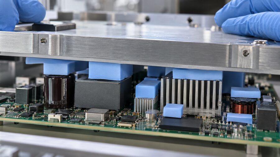
Gap fillers replace insulating air between a hot component and a cooling surface. Air conducts heat at only about 0.026 W/m·K near room temperature. A filled polymer usually conducts far better, although contact, pressure, and thickness still shape the result.
Für vorgeformte Wärmeleitpads, the supplier provides a nominal sheet thickness. The pad becomes thinner when the assembly closes. For a dispensable material, the hardware usually sets the final thickness.
| Begriff | What it means | Warum es wichtig ist |
| Nenndicke | Stated thickness of an uncompressed pad | Used to order the pad |
| Supplied thickness range | Thinnest and thickest pad allowed by manufacturing tolerance | Changes compression extremes |
| Zusammengefügte Lücke | Distance between surfaces after fastening | Usually sets installed thickness |
| Bond line thickness, or BLT | Final TIM layer between the surfaces | Shapes interface resistance |
Why a Dispensed Gap Filler Has No Sheet Thickness
A flüssiger Spaltfüller is deposited as a bead. The parts close to their stops and the material spreads through the available space. The assembled gap becomes its bond line.
Do not put a liquid filler’s “compression percentage” into a pad formula. Check its supported gap range, dispense volume, rheology, cure, and retention. Too little leaves dry areas; too much can flood keep-outs.
Start With a Gap Range, Not One Comfortable Number
The nominal CAD dimension helps during concept work, but release needs a tolerance stack. Include:
- Component body and solder-joint height
- PCB thickness, bow, and twist
- Heat sink, cold plate, or casting flatness
- Housing and boss tolerances
- Screw torque, sequence, and standoff height
- Coatings and insulation layers
- Pad thickness tolerance and thermal expansion
Record the minimum, nominal, and maximum assembled gap. For a wide interface, map the area too. A housing can be 1.2 mm away at one corner and 1.7 mm at another. An average hides that tilt rather neatly.
Measure the Hardware Without Fooling Yourself
Use tolerance analysis early, then measure representative parts. Possible methods include CMM, optical height mapping, a height gauge, controlled witness material, cross-sectioning, or pressure film. A trial build can reveal the contact pattern.
An ordinary caliper can squeeze a soft pad and under-report its free thickness. Use the supplier’s method or a defined low-force gauge. Record the measurement force and sample condition. Also measure more than one “golden sample.” Production variation is less polite.

Calculate a Pad Thickness That Covers Both Extremes
For a preformed pad, compression is: C=\frac{T_0-G}{T_0}\times100%
Here, (T_0) is the uncompressed pad thickness and (G) is the assembled gap. If the gap is 1.5 mm and a 2.0 mm pad closes to that gap, the nominal compression is 25%.
You can reverse the equation for a first estimate: T_0=\frac{G}{1-C}
That calculation describes one point, not the tolerance range. For a pad-only workflow, see Auswahl der Dicke des Wärmeleitpads.
Check the Full Tolerance Window
Let the supplied pad range from (T_{min}) to (T_{max}). Let the assembled hardware gap range from (G_{min}) to (G_{max}).
The lowest compression occurs when the thinnest permitted pad meets the largest gap:
C_{low}=\frac{T_{min}-G_{max}}{T_{min}}
The highest compression occurs when the thickest permitted pad meets the smallest gap:
C_{high}=\frac{T_{max}-G_{min}}{T_{max}}
A candidate passes this screen only when (C_{low}) stays above the grade’s minimum and (C_{high}) below its maximum. Broad online percentages are hints, not design rules.
Worked Example: A 2.0 mm Pad Across a 1.4–1.7 mm Gap
Suppose the drawing and measurements produce the following hypothetical case:
| Input | Value |
| Nominal pad thickness | 2.0 mm |
| Supplied pad tolerance | ±0.1 mm |
| Pad thickness range | 1.9–2.1 mm |
| Assembled gap range | 1.4–1.7 mm |
| Supplier-approved compression window for this example grade | 10%–35% |
At the largest gap with the thinnest pad: C_{low}=\frac{1.9-1.7}{1.9}=10.5%
At the smallest gap with the thickest pad: C_{high}=\frac{2.1-1.4}{2.1}=33.3%
The candidate covers the geometric window. It still needs force, thermal, insulation, assembly, and reliability testing.

Compression Percentage Is Not the Same as Safe Assembly Force
Two pads can reach 30% compression and push back with very different forces. Formulation, reinforcement, thickness, temperature, and area all matter. Shore 00 hardness cannot replace a compression-deflection curve.
Ask for pressure versus deflection data for the actual grade and thickness. Convert that pressure into total load across the contact area.
Pressing one thumb into a kitchen sponge is easy. Pressing a whole tray of it by the same distance needs far more force. Large battery plates behave in the same, slightly annoying way.
Check the load against package limits, solder joints, board strain, fasteners, and housing distortion. Four screws around a large pad can create high corner pressure and weak contact in the middle.
If force is too high, consider a softer or thinner grade, divided pads, a mechanical redesign, or a low-modulus liquid filler. More screw torque is rarely a clever thermal strategy.

The Thinnest Reliable Bond Line Usually Wins Thermally
The bulk resistance of a uniform material layer can be screened with:
R_{material}=\frac{t}{kA}
Here, (t) is final thickness, (k) is through-plane conductivity, and (A) is heat-transfer area. All else equal, a thicker layer adds resistance.
The joint also includes contact resistance. A thin pad touching half the surface can lose to a slightly thicker material that wets both sides. Target the thinnest reliable bond line, not the smallest spreadsheet number.
Sehen Sie wie bond line thickness changes thermal performance and why thermal conductivity differs from thermal impedance before comparing datasheets.
Das Würth WE-TGF user guide plots impedance against thickness under a stated load for one family. Useful, yes—but not a curve for every pad on the market.

Choose the Material Format Around Geometry and Production
First fit the material format to the assembly. A Laird selection paper highlights related factors such as compressibility, dielectric behavior, silicone restrictions, and stability.
| Materialformat | How thickness is controlled | Good fit | Main watch item |
| Soft gap pad | Sheet thickness plus compression | Defined area and clean placement | Force and compression set |
| Reinforced pad | Carrier-supported sheet plus compression | Thin parts needing handling strength | Carrier can raise force or impedance |
| Wärmeleitpaste | Hardware gap plus deposited amount | Uneven or multi-height regions | Migration, residue, and volume |
| Einkomponentiges Gel | Stops, bead geometry, and closure | Low-stress automated assembly | Slump, storage, and voids |
| Two-part liquid filler | Stops, mixed volume, flow, and cure | Large areas needing retention | Mix ratio, air, cure, and cleanup |
When a Pad Is the Cleaner Choice
A pad is a visible, countable part. It can be die-cut around keep-outs and inspected before closure. That suits controlled gaps with adequate assembly force.
Pads also suit field replacement when the original grade is known. Do not infer thickness from a crushed, aged pad alone; compression set and removal can change it.
When Putty, Gel, or Liquid Filler Handles Tolerance Better
Highly conformable Thermische Klebemasse follows different component heights with less spring force. Gels and cure-in-place fillers add scalable dispensing.
These formats fit cast housings, batteries, power electronics, and multi-component boards. Still, “dispensable” does not mean self-correcting. Control mass, bead path, closure, venting, and inspection. A generous blob may trap air or enter a connector. Bit awkward, that.
Thickness Priorities Change by Application
| Anwendung | Dominant thickness concern | Practical direction |
| EV battery to cold plate | Large-area total force | Map the gap; compare low-modulus pad and liquid options |
| Wechselrichter oder Leistungsmodul | Hot spots, isolation, and flatness | Control BLT; test dielectric performance after aging |
| Outdoor 5G radio | Casting tolerance, vibration, and service | Compare zoned pads with stable gel or putty |
| AI server accelerator | Heat flux, cold-plate flatness, and board strain | Minimize reliable BLT; map pressure |
| LED board to housing | Uniformity and optical cleanliness | Screen bleed and volatile residue |
| GPU or VRAM repair | Unknown original grade and hardness | Use model-specific evidence and contact marks |
| Industriesteuerung | Variable castings and long life | Favor a wide validated process window |
A 1.5 mm gap below a regulator is not equivalent to 1.5 mm across a battery plate. Area, stiffness, voltage, orientation, and life change the answer.
What Goes Wrong When Thickness Is Off
| Beobachtetes Problem | Likely thickness-related cause | Useful correction |
| Partial witness mark | Too thin, too stiff, or gap larger than expected | Re-map the gap; screen a thicker or softer grade |
| PCB bow or package stress | Too thick or too much force | Check worst-case load; change grade or geometry |
| Unexpected high temperature | Excess BLT, poor contact, or voids | Measure BLT; test at realistic pressure |
| Pad extrudes or tears | Over-compression or shear during closure | Reduce deflection or revise assembly motion |
| Liquid enters keep-outs | Excess deposit or uncontrolled flow | Adjust volume, bead, venting, or closure |
| Drift after cycling | Compression set, pump-out, slump, or contact loss | Age joints; recheck temperature and coverage |
| Serienstreuung | Uncontrolled gap, torque, pad, or dispense | Test process capability at both extremes |
Stacking pads is not a dependable cure for an unknown gap. It adds a contact boundary and allows slip. If unavoidable, qualify the stack as a new construction.
Validate the Thickness Before Production Release
No standard selects the thickness for you. Standards control a measurement or exposure; the product still needs pass-fail limits.
At material level, check:
- Thickness under a stated measurement force
- Compression-deflection at relevant thickness and temperature
- Thermal impedance at realistic BLT and pressure
- Dielectric behavior when the TIM provides insulation
- Rheology, mix ratio, cure, and void sensitivity for liquids
- Compression set or stress relaxation
ASTM D5470 is widely used for thermal transmission properties of suitable TIM specimens. Check pressure, thickness, area, temperature, and conditioning before comparing data. The result does not automatically predict device temperature.
Haktak also summarizes Gängige TIM-Prüfnormen for interface and bulk-property screening.
Test representative assemblies at both gap extremes. Check coverage, torque, pressure, board strain, device temperature, voids, dispense mass, and rework. Repeat functional measurements after aging.
Relevant exposures may include IEC 60068-2-14 temperature change, IEC 60068-2-64 random vibration, or ISO 16750-3 and -4 automotive conditions. UL 94 classification must match the grade and tested thickness. None replaces system-level electrical safety review.

Give the Supplier These Inputs, Not Just “I Need 2 mm”
A useful request includes:
- Minimum, nominal, and maximum gap; height map for large areas
- Contact area, surfaces, flatness, and heat load
- Clamp force, torque, stops, and component load limits
- Voltage, insulation, clearance, and flammability needs
- Temperature, vibration, fluids, and target life
- Placement or dispensing method, rate, inspection, and rework
With those inputs, Materialauswahl und Prüfungsunterstützung can narrow candidates before samples reach the line. That beats ordering three random thicknesses and hoping one behaves.
Fazit
The right gap filler is not the thickest material that touches under nominal conditions. It is the thinnest validated system that maintains contact across the real gap range without exceeding mechanical, thermal, electrical, process, or reliability limits.
For pads, calculate compression at both tolerance extremes and then verify force. For putties, gels, and liquid fillers, control final bond line through hardware stops, dispense volume, flow, and cure. In both cases, finish the decision in representative hardware—not on a datasheet alone.
Häufig gestellte Fragen
How thick should a thermal gap filler be?
There is no universal value. Choose the thinnest material that covers the gap range while meeting the grade’s force and thermal limits. For liquids, select a supported bond line range.
How do I measure the gap for a thermal pad or gap filler?
Build a tolerance stack, then measure representative assemblies. CMM, optical mapping, controlled witness material, height gauges, or cross-sectioning may help. Record the extremes, not just an average.
What compression ratio should I use for a gap pad?
Use the supplier’s range for the exact grade and thickness. Confirm force-deflection data too, because an acceptable percentage can still create excessive load.
What happens if a thermal pad is too thick?
It can add resistance, bow the PCB, overload packages or solder joints, distort the housing, or extrude from the joint.
What happens if a thermal pad is too thin?
It may not contact both surfaces at the largest gap. Air pockets then raise resistance and create hot spots or unit variation.
Can I stack two thermal pads to fill a larger gap?
Avoid it when one qualified pad is available. A stack adds an interface and can slip. If required, qualify the complete construction for resistance, load, and aging.
Do different component heights need different pad thicknesses?
Often, yes. Zoned pads can match height groups. Across many uneven components, putty or gel may reduce force and part count, but flow still needs control.
How do I choose thickness for thermal putty, gel, or liquid gap filler?
Define the bond line range set by the hardware and confirm material support. Control dispense volume, spread, voids, overflow, cure, orientation, and aged retention.
Can higher thermal conductivity compensate for a thicker gap filler?
Sometimes in a bulk calculation, but not automatically in the joint. Contact, pressure, and BLT matter. Compare impedance under similar conditions and verify device temperature.
How should gap filler thickness be validated before mass production?
Test both gap extremes with production-intent parts. Measure contact, force or strain, temperature, BLT or compression, and unit variation. Repeat key checks after relevant aging.