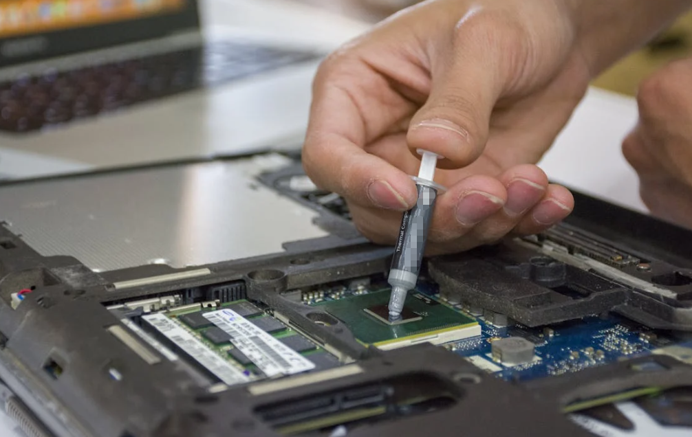
An outdoor sensor comes back from the field with corrosion around a connector. The obvious thought is, “Let’s pour resin over the whole board.” Maybe that works. Or maybe the resin traps heat around a regulator, cracks a solder joint when it cures, and makes the next failure impossible to repair.
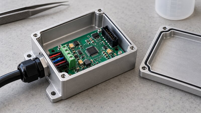
That is the odd thing about potting. It can protect electronics remarkably well, but it commits the entire assembly to the choice. You are designing a new part around the PCB, in effect. This guide walks through that decision: when potting makes sense, which chemistry to try, how to fill a cavity without hidden problems, and what to test before production.
What a potting compound does inside an electronic enclosure
In electronic potting, a liquid compound flows into a housing or defined cavity around components. It then cures or sets into a solid or gel-like mass. The resulting encapsulant can help keep moisture and contaminants away from sensitive areas, restrain parts under vibration, and provide electrical insulation where the complete design supports it. Certain formulations can also move heat toward a housing or cooling surface.
Das Wort encapsulation is sometimes used for the same process. More narrowly, it can mean covering a selected component or section instead of filling a whole enclosure. Define the physical coverage in your drawing; the label alone is too vague.
Potting does have limits. Resin cannot make a badly designed cable entry watertight. It cannot turn a hot plastic box into a heat sink. It cannot make a failed PCB easy to repair. Picture filling a suitcase with expanding foam: its contents stay put, but reaching one loose wire afterward becomes quite a job.
| Protection method | What goes onto the assembly | Useful when | Hauptkompromiss |
|---|---|---|---|
| Full potting | Bulk resin fills an enclosure or deep cavity | The module needs extensive environmental or mechanical protection | Mass, cure stress, heat-path change and limited repair |
| Local encapsulation | Compound covers one part or a selected board zone | A coil, sensor or high-risk area needs targeted protection | The transition edge and unprotected areas need design |
| Schutzlack | Thin film follows board surfaces | Surface contamination protection with less weight and better access | Little structural support; coverage and masking matter |
| Gasket or perimeter seal | Seal around enclosure joints | The housing needs a defined external barrier and service access | Joint geometry, compression and cable entries decide sealing |
| Wärmeleitpad | Soft interface between a hot part and cooler | Heat must cross an uneven gap | Usually does not protect or encapsulate the whole board |
This comparison matters early. A manufacturer may be able to solve the actual failure with a gasket, selective coating, or local fill. If the design truly needs bulk protection, HAKTAK’s electronic adhesives and protection materials provide a useful map of neighboring functions. Do not ask one material to do every job by accident.
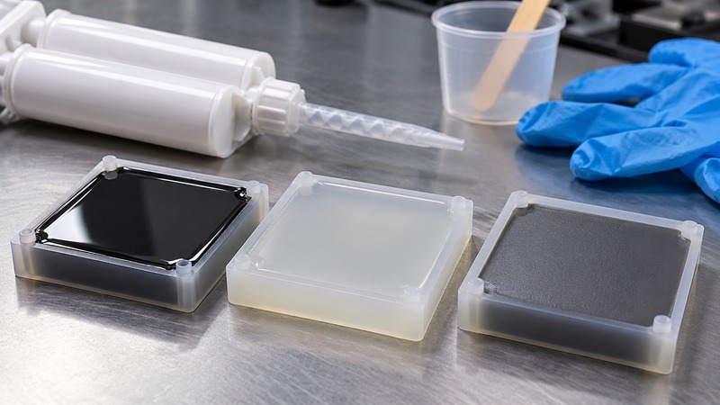
Epoxy, silicone or polyurethane: start with what might fail
These are three common starting families, not three fixed sets of properties. Formulation, filler, cure mechanism and hardness can change the outcome within each family. Before choosing a chemistry, write down the assembly’s likely failure: water at a seam, a heavy part shaking loose, a solder joint stressed by thermal expansion, or a hot device with no route to the case.
Epoxy: strength with a stress bill attached
Epoxy potting often suits applications needing a tougher cured mass, good adhesion and chemical resistance. Think of a transformer or rugged industrial module where a rigid body helps hold components in place. Some grades can be filled for thermal transfer; others are primarily protective. Never infer heat transfer from the word Epoxidharz.
Rigidity brings a cost. During cure, the compound may shrink and release heat. Later, the resin, PCB, tall components and metal housing expand by different amounts. A stiff mass can transfer that movement into solder joints or fragile packages. For a board with large ceramic capacitors, a hard grade that survives a simple pull test might still be the wrong long-term choice.
A deep pour changes the cure
The temperature reached inside a large casting can be higher than in a thin laboratory sample. Mix ratio, fill volume, geometry, ambient conditions and the manufacturer’s permitted pour depth all matter. Don’t assume a resin that cures safely in a small cup will behave the same way in a thick, insulated housing. Ask for exotherm and section-thickness guidance for the exact grade.
Silicone: softer protection for a moving assembly
Silicone potting systems can remain compliant after cure, which helps when a product sees wide temperature swings or contains delicate parts. A soft gel may place less mechanical load on a tall component than a rigid casting. It can be a good screening candidate for outdoor electronics, lighting and sensor modules.
You still need to check adhesion to the actual housing, surface cleanliness, cure inhibition, tear behavior, and any restrictions on silicone-related residues near contacts, optics, coatings or later bonding. A silicone family name is not proof of those details. Condensation and addition cure systems also have different processing behavior; use the supplier’s instructions for the specific grade.
Polyurethane: a useful middle ground, with its own limits
Polyurethane, often called PU or urethane, is another option when some flexibility and mechanical protection are needed together. Its feel after cure may sit between a soft silicone and a hard epoxy, though formulations vary a lot. It is worth screening for industrial controls, sensors and modules exposed to vibration.
Check moisture sensitivity during storage and processing, resistance to the actual oils or cleaners in service, and behavior at both the hot and cold limits. A “flexible PU” description tells you too little about a washdown cabinet or an outdoor device that freezes overnight.
| The dominant need | Chemistry worth screening first | Evidence that could change your mind |
|---|---|---|
| Rigid support and exposure to specified chemicals | Epoxidharz | Cured modulus, shrinkage, exotherm, adhesion and cycling failures |
| Low stress around delicate parts and wide thermal cycles | Silikon | Adhesion, contamination restrictions, tear resistance and cure behavior |
| Flexible protection for an industrial assembly | Polyurethan | Moisture control, chemical compatibility and temperature limit |
| Protection plus a path for heat to escape | A qualified thermally filled formulation in the suitable family | Viscosity, real heat path, component temperature and full-cavity cure |
Use the table to pick two or three candidates for trials. There is no universal winner. Browse the electronic material product directory by function and chemistry, then verify that a listed grade is actually suitable for the required cavity fill and cure depth. A small sealing adhesive, for example, is not automatically a full-depth potting compound.
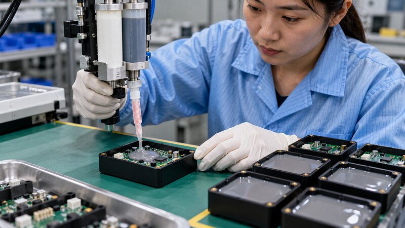
Design the cavity before choosing the resin
The housing is part of the process. Measure its usable volume and deepest section. Identify where air can escape as liquid flows around a connector, transformer, or board standoff. A blind pocket under a component is an invitation to keep a bubble. Vents and a deliberate fill path are often more useful than simply pouring faster.
Mark keep-out areas on the drawing. Connectors, switches, trim points, pressure ports, optical windows, vents, and test pads may need to stay clear. Consider cable jackets, seals, solder mask, plastics and metal coatings as real substrates. Surface adhesion that looks strong on bare aluminum may not match an actual coated enclosure.
Then ask what happens if a unit fails in the field. Can the whole potted module be replaced? Does a technician need access to a fuse or connector? A softer material might be removable in a local area, but “reworkable” should mean a documented method that leaves the device intact. Hardened epoxy may turn diagnosis into a destructive teardown.
Here is a simple case. A factory sensor has a small PCB, a metal housing and a cable leaving through one wall. The PCB itself might survive a humidity test, while water enters along the cable-to-housing interface. Filling the cavity may help protect the board, but the cable seal still needs its own design and test. The production drawing must specify fill height, cable position, venting, and what remains exposed. HAKTAK’s industrial electronics application overview places those enclosure and material decisions in the context of sensors, controllers and power supplies.
Weight deserves a line in the brief, too. A resin-filled device is heavier. That may matter in a handheld instrument, drone, moving arm, or ceiling-mounted luminaire. Prototype the actual filled part instead of judging a neat empty housing.
Separate electrical, environmental and thermal requirements
“Protects electronics” covers three different tests. Keep them separate in the specification so a good result in one does not quietly stand in for the others.
Electrical insulation belongs to the finished design
Ask for dielectric and resistivity data on the exact cured formulation, with specimen thickness, conditioning and test method. Then review the voltage, geometry, void risk, aging and insulation system of the finished assembly. A bubble in a high-field area is more than a cosmetic mark. A potting data sheet cannot, by itself, approve the creepage and clearance strategy.
IEC 60664-1 addresses insulation coordination for low-voltage equipment within its defined scope, including requirements used to determine clearances, creepage and criteria for solid insulation. The applicable end-product standard and safety team decide how it applies to the actual device. Do not assume that pouring material over conductors automatically permits smaller spacing.
A waterproof resin does not grant an IP rating
A compound may resist moisture while water still enters at a connector, seam, cable gland or exposed interface. IEC 60529 classifies degrees of protection provided by enclosures. An IP rating belongs to the tested construction under the relevant conditions, not to a bucket of resin. Test the completed unit in its assembled state.
Likewise, a requested UL 94 material flammability classification concerns how a tested material specimen responds to a small-scale flame. UL’s material-testing overview explains the material context. A quoted V-0 rating is not the same as a finished-product fire approval, and it must be documented for the actual formulation and relevant thickness.
Heat needs somewhere to go
Potting replaces internal air with a solid or gel, but that alone does not guarantee cooler electronics. A power device still needs a path from its hot surface through the compound and housing to ambient air or a dedicated cooler. A thick layer of unfilled resin may add thermal resistance. A thermally filled material can help when it makes good contact with a heat-rejecting surface, but high filler loading may also make the liquid harder to dispense into tight spaces.
Measure the temperature of the actual hot parts before and after potting at the intended load and ambient. If thermal transfer is a principal requirement, use HAKTAK’s thermally conductive potting guide for the deeper discussion of filled formulations. This general guide stays focused on deciding whether and how to encapsulate.
Build a repeatable process, from clean PCB to full cure
Potting usually happens late in assembly. That is sensible: once the resin cures, inspecting or repairing a hidden joint becomes harder. Finish soldering, inspect the board, run the planned functional test, and prepare the surfaces before filling. Clean and dry according to the approved process. Trapped flux residue or moisture can become a problem you have sealed in permanently.
For a two-part material, control the A:B ratio, container condition, mixing method, pot life, and dispensing temperature. “Two equal-looking squirts” is not a process specification. A meter-mix system needs checks for ratio drift, mixer condition and air intake. Manual batches need their own weighing, mixing and traceability rules. HAKTAK’s Unterstützung des Ausgabeprozesses covers the move from a careful bench pour to a stable production fill.
Give air a route out
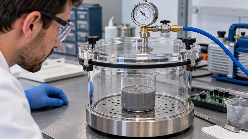
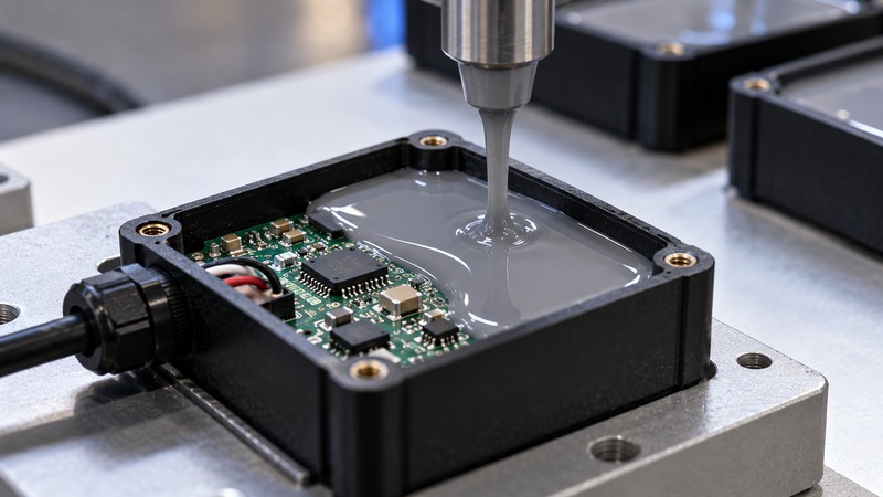
Dispense at a controlled location and rate so the resin advances through the cavity instead of closing over an air pocket. An angled fixture or staged fill may help a difficult geometry. Some materials and assemblies benefit from vacuum degassing, vacuum potting or pressure steps. These are process options to validate, not blanket requirements. Too aggressive a vacuum can cause other trouble, including foaming or movement of the assembly.
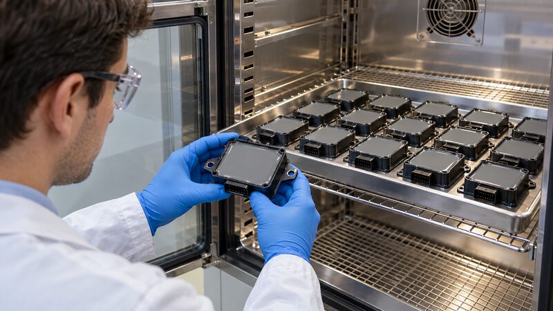
Fill height and cure schedule belong in the work instruction. The unit must reach the required cure state in its deepest section before final testing or packing. A warm outer surface does not tell you what happened in the center. If cure generates significant heat, confirm that components, housing and cable materials stay within their permitted exposure during the real pour.
| Build symptom | First questions | A sensible trial |
|---|---|---|
| Bubbles beside tall components | Is there a trapped pocket or no vent path? | Change fill direction or fixture angle; inspect a sectioned trial unit. |
| Soft or sticky patch after cure | Did the mix ratio, mixing quality or cure temperature drift? | Check metering records and a witness sample from the same batch. |
| Cracked package or lifted solder joint | Was the cured material too stiff, or did cure heat and shrinkage add stress? | Compare a lower-stress formulation and the actual cure profile. |
| Resin leaks onto a connector | Is the keep-out, seal or fill volume incomplete? | Add a physical barrier and revise the fill-height control. |
| Hotter regulator after potting | Did the resin block airflow or fail to reach a useful heat sink? | Measure the whole heat path; change the thermal design or material format. |
Inspection may include fill mass, visible coverage, surface cure, witness samples, electrical function and selected destructive sections. Choose checks that reveal the failures you care about. Looking only at the smooth top surface can miss a large pocket underneath a transformer.
When potting is the wrong solution
Full potting makes little sense when component-level service is part of normal maintenance. A gasketed housing plus selective coating may preserve access while meeting the real environmental requirement. That choice still needs its own ingress and aging tests, of course.
It can also be a poor fit for an assembly with no workable heat path, tight weight limits, or components that cannot tolerate cure temperature or mechanical restraint. Battery cells need particular care around swelling, venting and safety architecture; do not bury a pack or cell simply because a BMS board needs protection. Scope the protected region instead.
Some designs need only a local dam and fill around one component or a perimeter seal at the enclosure joint. Smaller coverage can lower resin volume, exotherm, mass and teardown pain. It does not make process control optional, but it may solve the actual problem with fewer side effects.
Send a useful supplier brief, then test the assembled device
Before asking for a grade, give the supplier the hardware story. Include the enclosure drawing, cavity volume and depth, substrates, exposed components, voltage, heat load, service environment and expected life. Add the target production rate, available cure time, rework policy and any material restrictions. If a previous compound failed, include photos and conditions; “it cracked” is a clue, not a full specification.
Request product-specific TDS and SDS information. Ask for viscosity under stated conditions, mix ratio, pot life, maximum pour guidance, full-cure schedule, cured hardness or modulus, adhesion, thermal properties where needed, electrical test conditions, and compatibility with your actual plastics, metals and cable jacket. If the requirements pull against one another, HAKTAK’s custom formulation support is an appropriate next step.
Make representative pilot units. Measure baseline electrical function and the temperature of hot components. Then run environmental exposure based on the device’s job: humidity or water entry, chemical contact, vibration, thermal cycling and powered aging as applicable. Repeat functional and insulation checks after exposure. Inspect or section selected units for hidden voids, cracks, delamination and corrosion. Set acceptance limits before testing, so the team is not debating them over a failed sample.
Das material selection and testing workflow can help organize that evidence. A data-sheet number starts the shortlist. The filled, cured, aged product makes the final call.
Fazit
A potting compound is more than liquid protection poured into a box. It changes the device’s heat path, weight, stress and repair plan. Start with the failure you need to prevent. Choose a chemistry and coverage that fit the assembly, give air and cure a controlled route, and validate the complete unit. Sometimes the right answer is full potting. Sometimes a small local fill or a better enclosure seal does the job with less fuss.
Häufig gestellte Fragen
1. What is a potting compound in electronics?
It is a flowable material placed around electronic components or into an enclosure, then cured or set to protect the assembly. The chosen formulation may provide environmental, mechanical, electrical or thermal functions. The finished performance depends on the whole device.
2. How is potting different from conformal coating?
Potting fills a cavity with a substantial mass of material. Conformal coating adds a thin film over selected board surfaces. Coating keeps weight down and usually preserves more access; potting can give greater bulk protection and support, with harder rework.
3. Which is better for a PCB: epoxy, silicone or polyurethane?
There is no universal best. Screen epoxy for rigid support and specific chemical exposure, silicone for lower mechanical stress, and PU for a needed balance of flexibility and protection. Verify the exact grade against the board, housing, environment and process.
4. Does potting make electronics waterproof or IP67?
Not by itself. Water may enter through connectors, cable entries or seams. An IP claim requires the relevant completed enclosure to be designed and tested under the applicable method. A resin property is only part of that story.
5. Can potting make a hot PCB run hotter?
Yes. It may block internal air movement or add a poor thermal path. A thermally filled grade can help only if heat reaches a useful housing or cooler. Compare actual component temperatures before and after potting at the intended load.
6. How do I prevent bubbles in potting resin?
Give displaced air an exit, control the fill direction and rate, and mix without pulling in extra air. Degassing or pressure methods may help certain material-and-cavity combinations. Inspect opened or sectioned trial units rather than judging only the surface.
7. Why can epoxy potting crack components?
Cure shrinkage, exotherm, rigid cured behavior and different rates of thermal expansion can load packages or solder joints. The risk depends on formulation and geometry. Compare stress after cure and thermal cycling, especially around tall or fragile parts.
8. Can I use ordinary two-part hardware-store epoxy?
Do not assume it is suitable. Electronic potting calls for documented cure depth, exotherm, electrical properties, compatibility and reliability. A general repair epoxy may have none of the evidence needed for the assembly.
9. Can potted electronics be repaired?
Sometimes a soft material can be removed locally, but any removal can damage components or conductors. Rigid epoxy often requires destructive work. Decide the service and replacement strategy before committing to full potting.
10. What should I test before mass production?
Build representative units with the real enclosure and process. Check mixing, full cure, coverage and voids; then measure electrical function, insulation and hot-part temperatures. Apply the relevant environmental and cycling profile, repeat those checks, and inspect selected interiors.