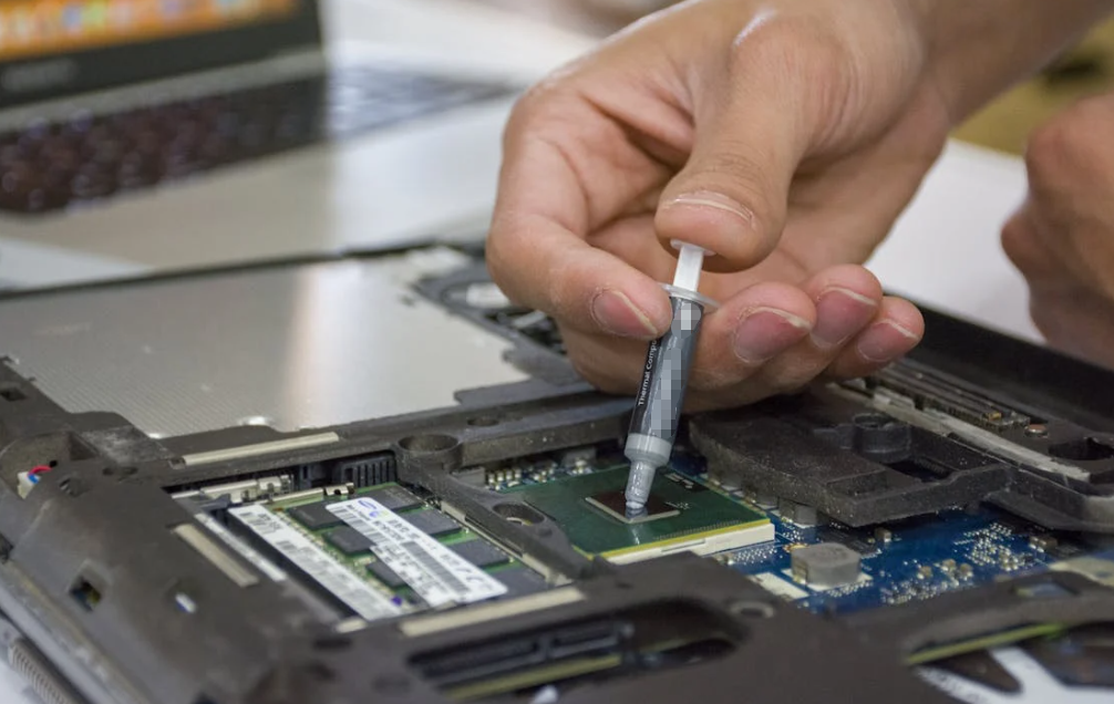
MOSFETs need thermal pads when heat must move from the package to a heat sink, metal housing, cold plate, or chassis, and the interface needs controlled thickness, gap filling, electrical insulation, or clean assembly. The right MOSFET thermal pad depends on power loss, contact area, package type, voltage isolation, gap size, compression force, pad hardness, dielectric strength, and thermal impedance.

For most power electronics, do not choose a MOSFET thermal pad by W/mK alone. A high-conductivity pad can still perform poorly if it is too thick, too hard, under-compressed, or unable to provide the required electrical isolation.
The better goal is simple: choose a pad that gives full contact, low thermal impedance, safe electrical isolation, and stable performance after heat cycling.
Why MOSFET Thermal Pads Matter
MOSFETs are common in power supplies, motor drives, EV electronics, battery systems, LED drivers, telecom power modules, and industrial controllers. They switch current. They also generate heat.
If that heat stays near the junction, the MOSFET runs hotter. Higher temperature can reduce efficiency and shorten device life. It can also increase thermal stress on solder joints, boards, and nearby parts.
A thermal pad helps move heat from the MOSFET package into a heat sink or housing. It also fills air gaps. Air is a poor thermal conductor, so even a small gap can hurt cooling.
Thermal pads are useful when the design needs:
- Gap filling
- Elektrische Isolierung
- Controlled thickness
- Clean assembly
- Die-cut shapes
- Lower mess than thermal grease
- Repeatable production
In MOSFET designs, the pad is not just a soft sheet. It is part of the thermal path and often part of the insulation system.
When Do MOSFETs Need Thermal Pads?
MOSFETs do not always need thermal pads. Some designs use thermal grease, soldered thermal vias, direct copper planes, clips, or metal-backed substrates. A pad is useful when the mechanical or electrical interface calls for it.
Use thermal pads for MOSFET heat sink contact
Use a thermal pad when the MOSFET package or board needs to transfer heat to a heat sink, metal cover, or enclosure wall across a small gap.
This is common when:
- The MOSFET is mounted near a metal housing
- The heat sink is not perfectly flat
- There is a known mechanical gap
- The design needs clean assembly
- The pad also provides electrical insulation
Use insulating thermal pads for MOSFETs when the tab is live
Many MOSFET packages have a drain-connected tab or exposed pad. If that surface touches a metal heat sink directly, it may create an electrical short.
An electrically insulating thermal pad can transfer heat while blocking current.
This matters when:
- Der Kühlkörper ist geerdet.
- The heat sink is shared by multiple devices
- The MOSFET tab is electrically live
- The enclosure is metal
- Safety isolation is required
For more detail, see HakTak’s guide Elektrisch isolierende Wärmeleitpads: Wann braucht man sie?.
Use thermal pads when gap tolerance is hard to control
PCB thickness, solder height, MOSFET package height, heat sink flatness, and housing tolerance all add up. A thermal pad can absorb some of that tolerance.
But the pad must be chosen carefully. Too thin, and it may not touch. Too thick, and it can stress the MOSFET or PCB.
MOSFET Thermal Pad vs Thermal Grease
Thermal grease and thermal pads both reduce thermal resistance. They do it in different ways.
Thermal grease is best for thin, flat, clamped interfaces. It can form a very thin bond line. But it does not hold parts in place and it can be messy.
Thermal pads are better when the interface needs gap filling, electrical insulation, fixed thickness, or cleaner assembly.
| Faktor | MOSFET Thermal Pad | Wärmeleitpaste |
| Gap filling | Better for controlled gaps | Poor for larger gaps |
| Strichformel-Kontrolle | Fixed by pad thickness and compression | Depends on amount and pressure |
| Elektrische Isolierung | Common in insulating grades | Depends on formulation |
| Überarbeiten | Often cleaner | Requires cleaning old grease |
| Montage | Easy to place | Can vary by operator |
| Best use | Heat sink gap, housing contact, insulation | Thin flat interface with clamping |
For grease application basics, see HakTak’s article Tips for Applying Thermal Grease and How It Works.
MOSFET Thermal Pad vs Thermal Putty
Thermal putty can be better than a pad when the gap is uneven or several components have different heights.
Thermal pads work best when the gap is known and repeatable. Putty works well when the gap is less predictable.
| Design Condition | Better Starting Point | Wärmeleitpaste |
| Flat controlled MOSFET-to-heat-sink gap | Wärmeleitpad | Poor for larger gaps |
| Multiple component heights | Thermal putty | Depends on amount and pressure |
| Need die-cut part | Wärmeleitpad | Depends on formulation |
| Low-pressure uneven housing | Thermal putty or soft gap filler | Requires cleaning old grease |
| Clean manual placement | Wärmeleitpad | Can vary by operator |
| Best use | Heat sink gap, housing contact, insulation | Thin flat interface with clamping |
For uneven interfaces, see HakTak’s article Wärmeleitpaste vs. Wärmeleitpad: Wie man bei ungleichmäßigen Spalten die richtige Wahl trifft.
How to choose a MOSFET thermal pad by power loss
Start with the heat. A MOSFET thermal pad only makes sense if it can move enough heat through the available area.
Estimate MOSFET power dissipation
Power loss may include:
- Conduction loss
- Switching loss
- Gate drive-related loss
- Reverse recovery-related loss
- Package and board spreading losses
For a simple first pass, engineers often start with total MOSFET loss in watts. Then they map that heat into the available thermal path.
Build a rough thermal path
A MOSFET thermal path may look like this:
- Junction
- Package case or exposed pad
- Wärmeleitpad
- Heat sink or housing
- Air or liquid cooling
Each step adds thermal resistance. The thermal pad is only one part, but it can still be a bottleneck.
Compare thermal impedance, not only W/mK
W/mK is useful. It is not enough.
Thermal impedance is closer to real interface behavior. It includes thickness, contact, and pressure effects.
ASTM D5470 is commonly used for thermal transmission properties of thermally conductive electrical insulation materials. ASTM states that this method measures steady-state thermal impedance and can be used for materials such as greases, phase change materials, gels, and soft or hard rubbers used in electronics heat transfer. Official reference: ASTM D5470.
HakTak also covers this topic in Wärmeleitfähigkeit vs. Wärmewiderstand bei der TIM-Auswahl.
How to choose insulating thermal pads for MOSFET heat sinks

Electrical isolation is often the main reason to choose a thermal pad for MOSFETs.
Check if the MOSFET tab or exposed pad is electrically live
Some MOSFET packages connect the drain to the tab. If that tab contacts a grounded heat sink, it can short the circuit.
Ask these questions:
- Is the MOSFET tab connected to drain?
- Is the heat sink grounded?
- Are several MOSFETs sharing one heat sink?
- Is the housing metal?
- Is there a safety isolation requirement?
If the answer is yes, an insulating thermal pad may be needed.
Check dielectric strength and breakdown voltage
Dielectric strength and breakdown voltage show how the material handles electrical stress.
ASTM D149 is a reference standard for dielectric breakdown voltage and dielectric strength of solid electrical insulating materials.
Do not look only at the nominal rating. Compression and final thickness matter. A pad that is over-compressed may have less dielectric margin than expected.
Balance insulation with thermal resistance
Thicker pads may improve electrical margin. They also increase thermal resistance.
The right choice is not the thickest insulating pad. It is the thinnest pad that fills the gap, meets dielectric needs, and keeps the MOSFET temperature under control.
Thermal pad thickness for MOSFETs
Thermal pad thickness is one of the most important choices.
Measure the MOSFET heat sink gap
Use real assembly data if possible. CAD is useful, but it misses tolerance stack-up.
Check:
- MOSFET package height
- PCB thickness
- Solder height
- Heat sink flatness
- Housing tolerance
- Screw torque variation
- Board bending
Measure minimum, nominal, and maximum gap.
Choose the thinnest pad that still fills the gap
A thinner pad usually gives lower thermal resistance. But it must still touch both surfaces at the maximum gap.
If it is too thin, it may not contact the heat sink. If it is too thick, it may stress the MOSFET or board.
HakTak’s guide Auswahl der Dicke von Wärmeleitpads für Elektronik gives a step-by-step method.
Check bond line thickness after compression
The final compressed thickness is the bond line thickness. That is the thickness heat must pass through.
For a simple interface:
R = t / (k × A)
Wo
- R ist thermischer Widerstand
- t is final thickness
- k ist Wärmeleitfähigkeit
- A Kontaktfläche
HakTak explains this in Wie sich die Dicke der Klebefuge auf die thermische Leistung auswirkt.
Thermal pad compression for MOSFETs

Thermal pads need compression. The right amount depends on pad hardness, thickness, and the mechanical design.
Too little compression leaves air gaps
Under-compression can cause:
- Poor contact
- High thermal resistance
- Hotspots
- Unstable temperature results
- Unit-to-unit variation
This can happen when the pad is too thin or too hard.
Too much compression can damage the MOSFET assembly
Over-compression can cause:
- Leiterplattenverbiegung
- Package stress
- Solder joint stress
- Housing deformation
- Kissenextrusion
- Lower dielectric margin
This is a real risk in MOSFET designs. The component may be small, but the stress can be local.
Calculate compression across the full gap range
Do not calculate compression only at nominal gap.
Check:
- Minimaler Abstand
- Nominale Lücke
- Maximale Lücke
HakTaks Artikel Wärmeleitpad-Kompressionsverhältnis: Wie viel ist genug? explains the method.
Soft vs hard thermal pads for MOSFETs
Hardness affects force and contact.
Soft pads compress more easily. They help when pressure is low or surfaces are uneven. Harder pads can be easier to handle and more dimensionally stable, but they need more force.
Choose soft MOSFET thermal pads for low-pressure designs
Soft pads are useful when:
- PCB bending must be limited
- The MOSFET package is fragile
- The housing is not very flat
- Screw force is low
- Gap tolerance is wider
Choose harder MOSFET thermal pads for controlled assemblies
Harder pads may be useful when:
- The gap is tightly controlled
- The heat sink is flat
- The assembly can apply enough pressure
- Die-cut handling matters
- Rework needs to be cleaner
ASTM D2240 is a reference for durometer hardness testing of rubber-like materials.
For a practical comparison, see HakTak’s article Weiche vs. harte Wärmeleitpads: Welche sind besser?.
MOSFET thermal pad selection table
| Selection Factor | What to Check | Why It Matters |
| Power loss | MOSFET heat in watts | Sets the thermal target |
| Contact area | Package or heat spreader area | Smaller area raises heat flux |
| Spannenbereich | Minimum, nominal, maximum | Controls pad thickness |
| Wärmeimpedanz | At real thickness and pressure | Better than W/mK alone |
| Durchschlagfestigkeit | Required voltage isolation | Prevents electrical breakdown |
| Pad hardness | Shore or durometer value | Controls compression force |
| Compression ratio | At min and max gap | Prevents poor contact or stress |
| Operating temperature | Continuous and peak | Prevents softening or aging |
| Druckverformungsrest | After heat and time | Maintains long-term contact |
| Rework behavior | Removal and residue | Affects serviceability |
Common MOSFET packages and thermal pad considerations
Different MOSFET packages create different thermal interface problems.
TO-220 and TO-247 MOSFET thermal pads
These packages often mount to a heat sink. Electrical isolation may be required if the tab is live. The pad must withstand mounting force and voltage stress.
Check:
- Durchschlagfestigkeit
- Polsterstärke
- Screw torque
- Case flatness
- Heat sink finish
H3: Surface-mount MOSFET thermal pads
Surface-mount MOSFETs often use PCB copper for heat spreading. A thermal pad may be used to connect the board or package area to a housing or heat spreader.
Check:
- Board warpage
- Component height
- Housing gap
- Low-pressure contact
- Soft pad options
MOSFET modules and power boards
Power boards may use several MOSFETs near one heat spreader. A pad can help isolate and transfer heat, but gap tolerance can be complex.
Check:
- Shared heat sink voltage risk
- Multi-device flatness
- Compression uniformity
- Hot spot risk
Testing MOSFET thermal pads before production
Testing should match the final assembly. A datasheet value is not enough.
Test thermal performance in the real MOSFET assembly
Measure:
- MOSFET case temperature
- Heat sink temperature
- Board temperature
- Umgebungstemperatur
- Load condition
- Thermal steady state
Use the actual screws, clips, housing, and pad thickness.
Test electrical insulation after compression
If the pad is insulating, test it after assembly or after equivalent compression. Final thickness matters.
Test aging and cycling
Power electronics do not sit at one temperature forever. Test:
- Temperaturwechselbeanspruchung
- Power cycling
- High-temperature aging
- Vibration
- Humidity if relevant
- Druckverformungsrest
For polymer thermal property testing, ISO 22007-2 covers the transient plane heat source method for thermal conductivity and diffusivity.
When a MOSFET thermal pad is not the best choice
Thermal pads are useful. They are not universal.
Use thermal grease for very thin, clamped MOSFET interfaces
If the MOSFET or module is tightly clamped to a flat heat sink and electrical insulation is handled another way, grease may give lower bond line thickness.
Use thermal putty for uneven MOSFET board gaps
If the MOSFET shares a housing gap with other components at different heights, putty may conform better than a fixed pad.
Use potting for protection and heat spreading
If the design needs encapsulation, moisture protection, and heat transfer through a volume, potting compound may be better than a pad.
Common mistakes when choosing MOSFET thermal pads
The first mistake is choosing only by W/mK. A high-W/mK pad can fail if it is too thick or does not contact well.
The second mistake is ignoring electrical isolation. A MOSFET tab may be live.
The third mistake is selecting thickness from nominal gap only. Always check min and max gap.
The fourth mistake is using a hard pad in a low-pressure assembly. It may not compress enough.
The fifth mistake is over-compressing the pad. This can stress the board and reduce dielectric margin.
The sixth mistake is skipping aging tests. Heat cycling can change pad contact over time.
The seventh mistake is assuming the same pad works for every MOSFET package.
HakTak perspective
At HakTak, MOSFET thermal pad selection starts with the real interface. A useful recommendation needs more than a target W/mK.
Engineers should provide:
- MOSFET package type
- Power loss or heat load
- Contact area
- Spannenbereich
- Heat sink or housing material
- Required dielectric strength
- Available pressure or screw torque
- Oberflächenebene
- Operating temperature range
- Thermal cycling requirement
- Vibration or shock requirement
- Rework expectation
- Produktionsprozess
With this information, HakTak can recommend pad thickness, hardness, conductivity grade, dielectric rating, and compression range.
The best MOSFET thermal pad is not always the highest-conductivity pad. It is the pad that keeps the MOSFET cool, isolated, and mechanically safe in the final product.
Fazit
Thermal pads for MOSFETs must solve several problems at the same time. They must move heat. They may need to insulate voltage. They must fill the gap. They must compress without damaging the assembly. They must also stay stable after heat, time, and cycling.
Start with the MOSFET’s power loss, package type, gap range, and voltage requirement. Then compare pad thickness, hardness, thermal impedance, dielectric strength, and reliability data.
Do not select by W/mK alone. The right MOSFET thermal pad is the one that performs well in the real assembly.
Häufig gestellte Fragen
Do MOSFETs need thermal pads?
MOSFETs need thermal pads when heat must move to a heat sink, housing, or chassis across a gap, especially when electrical insulation or clean assembly is required.
What is the best thermal pad for MOSFETs?
The best pad depends on power loss, gap size, contact area, voltage isolation, pressure, thickness, hardness, and reliability requirements.
Should I use thermal grease or thermal pad for MOSFETs?
Use grease for thin, flat, clamped interfaces. Use a pad when you need gap filling, controlled thickness, insulation, or cleaner assembly.
Do MOSFET thermal pads need electrical insulation?
Often yes. If the MOSFET tab or exposed pad is electrically live and the heat sink is conductive, an insulating thermal pad may be needed.
How thick should a MOSFET thermal pad be?
It should be thick enough to fill the maximum gap and thin enough to keep thermal resistance low. Check compression at minimum, nominal, and maximum gap.
Is higher W/mK always better for MOSFET thermal pads?
No. Thermal impedance, thickness, contact pressure, and insulation are often more important than W/mK alone.
How much compression does a MOSFET thermal pad need?
Enough compression is needed to make full contact without bending the PCB, stressing the package, or reducing dielectric margin.
Can thermal putty replace a MOSFET thermal pad?
It can in uneven or multi-height assemblies. For controlled flat gaps, a die-cut thermal pad is often cleaner and more repeatable.
What should be tested before production?
Test MOSFET temperature, heat sink temperature, thermal impedance, dielectric strength after compression, thermal cycling, vibration, and aging.
What data should I send to a thermal pad supplier?
Send package type, heat load, contact area, gap range, voltage isolation need, pressure limit, temperature range, and reliability conditions.