
You replace a 0.5 mm electrical insulation sheet with a 1 mm sheet. Same material family. Same listed thermal conductivity. Yet your power device runs hotter. So did the thicker sheet somehow lose conductivity?

Usually, no. The material’s thermal conductivity describes how readily heat moves through the material. Thickness tells you how far the heat must travel. Double that distance, with everything else equal, and you roughly double the sheet’s bulk thermal resistance. The material’s conductivity does not automatically change.
There is a catch, though. An electrical insulation sheet lives between real parts, not between perfectly flat diagrams. Contact pressure, surface shape, compressed thickness and electrical safety can change the choice. Let’s sort out those pieces before picking a thickness.
Here, electrical insulation means stopping unwanted current while allowing heat to reach a heat sink or housing. It is different from a thermal insulation pad, whose job is to block heat from reaching something else.
Three numbers that look alike but answer different questions
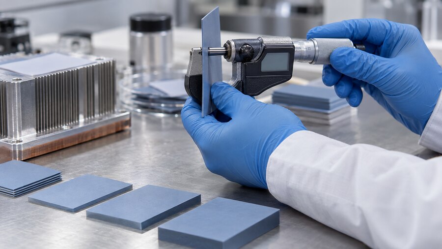
Thermal conductivity: a property of the material
Thermal conductivity, usually written k, describes heat movement through a material. Its unit is watts per meter-kelvin, or W/m·K. For a sheet between a transistor and a heat sink, the relevant direction is usually through the thickness, sometimes called through-plane conductivity.
That last phrase matters. A layered sheet may spread heat quite well along its face but move heat less well from one face to the other. If a supplier offers only an in-plane value, ask for the through-plane result before using it in a stack calculation.
For an unchanged, reasonably uniform formulation tested under similar conditions, a 0.5 mm sheet and a 1 mm sheet can carry the same listed k. A different filler blend, carrier film, adhesive layer or test method can produce a different value. Thickness alone isn’t the whole explanation.
Thermal resistance: the obstacle along the heat path
Thermal resistance describes the temperature rise per watt through a particular piece or heat path. Its unit is K/W. It depends on thickness, k and contact area. A test report may give an area-normalized thermal impedance in °C·in²/W or K·cm²/W. Unlike a bare k value, a measured impedance may include the effects of contact at the two faces, depending on the method and setup.
When you compare supplier data, check whether you are looking at material conductivity, calculated bulk resistance or measured interface impedance. For a deeper walk-through, HAKTAK’s guide to thermal conductivity versus thermal impedance tackles that distinction in TIM selection.
Dielectric properties: what happens to the electricity
An electrical insulator needs an electrical specification too. Breakdown voltage, usually given in kV or V, is the voltage at which a tested specimen fails under stated conditions. Dielectric strength expresses breakdown relative to specimen thickness, often in kV/mm. Volume resistivity describes resistance to current through the material. None of these numbers tells you its thermal resistance.
| Data-sheet term | Typical unit | What to check before comparing sheets |
| Thermal conductivity, k | W/m·K | Through-plane or in-plane? Which test and temperature? |
| Supplied thickness | mm | Is this before clamping? What is the tolerance? |
| Installed thickness | mm | What thickness remains at the actual pressure and gap? |
| Bulk thermal resistance | K/W | Is contact area included in the calculation? |
| Measured thermal impedance | K·cm²/W or °C·in²/W | Which thickness, pressure and surface condition were tested? |
| Dielectric breakdown voltage | V or kV | What specimen thickness, frequency, electrodes and conditioning? |
Those are six separate questions, not six names for the same performance score.

What is the relationship between thermal conductivity and electrical insulation sheet thickness?
For steady heat flow through a simple, uniform sheet:
R<sub>bulk</sub> = t / (k × A)
Here, t is the sheet’s installed thickness in meters, k is through-plane thermal conductivity in W/m·K and A is the effective heat-flow area in square meters. The result is K/W. If you want resistance per unit area, multiply by area: R”<sub>bulk</sub> = t/k, in m²·K/W.
It’s a little like walking through a corridor. The flooring has not become harder to walk on when the corridor gets longer. You simply have farther to go. A thicker layer makes a longer heat path.
Say the same hypothetical material has k = 2 W/m·K and the heat-flow area is 1 cm². Ignore the two contacts for this example:
| Installed thickness | Same material k | Calculated bulk resistance over 1 cm² |
| 0.25 mm | 2 W/m·K | 1.25 K/W |
| 0.50 mm | 2 W/m·K | 2.50 K/W |
| 1.00 mm | 2 W/m·K | 5.00 K/W |
The numbers are illustrative calculations, not product ratings. If 10 W of heat crossed only that ideal 1 cm² path, changing from 0.5 to 1.0 mm would add 25 K of temperature drop across the bulk sheet in this simplified model. A real device has spreading resistance, other heat paths and changing temperatures. You cannot use that 25 K as a prediction for every MOSFET or inverter.
Flip the comparison. At the same thickness and area, doubling k from 2 to 4 W/m·K halves the calculated bulk resistance. But a 4 W/m·K sheet at twice the thickness gives the same ideal bulk result as a 2 W/m·K sheet at the thinner thickness. This is why picking the largest W/m·K number in a catalog can be oddly unhelpful.
Why measured apparent conductivity may vary with thickness
Now for the part that causes arguments in design reviews. Many commercial sheets are composites: a polymer loaded with ceramic particles, possibly with a woven reinforcement, polyimide film, adhesive or other layers. You may see apparent thermal conductivity rather than the intrinsic k of a perfectly homogeneous material.
When a tester clamps a sample, heat crosses the top contact, the sheet and the bottom contact. A useful first approximation is:
R<sub>total</sub> ≈ R<sub>contact,top</sub> + t/(k × A) + R<sub>contact,bottom</sub>
If contact losses are large relative to a very thin specimen, calculating k from one thickness can distort the result. The official ASTM D5470-17(2024) test method discusses measuring thermal impedance at several thicknesses to separate apparent conductivity from the contact contribution. It also notes that the term apparent is appropriate for heterogeneous electrical insulators.
Construction can matter as much as the test fixture. Add a film carrier, change filler orientation or compress the pad differently, and you have changed the finished heat path. At extremely small film scales, thickness-related transport effects can also arise. That is a different situation from cutting two ordinary sheets of the same formulation at different gauges. Keep the comparison tied to the actual grade and finished construction.
Why the thinnest sheet may run hotter
Imagine laying a thin plank across a stream. If it doesn’t reach the far bank, it doesn’t matter how good the plank material is. Likewise, an insulation sheet that does not touch both faces cannot provide a reliable heat path.
Consider a lid that bows slightly over a power board. The gap at one corner is 0.35 mm; at another, 0.65 mm. A 0.5 mm pad may look like the lower-resistance choice on paper. At the 0.65 mm corner, it may barely touch—or leave air behind. A somewhat thicker, soft pad could work better there because it contacts both surfaces. At the 0.35 mm corner, however, that same thicker pad might need more force than the device can tolerate. There is no free lunch.
This is why you should measure minimum and maximum assembled gap, not just the drawing’s nominal gap. HAKTAK’s guide on how to select thermal pad thickness lays out that tolerance workflow. The detail to carry into this article is simple: the heat sees the compressed thickness during operation, not the number printed on the unopened sheet’s label.
Pressure helps a soft interface fill surface valleys. Too little pressure leaves contact patches and trapped air. Too much pressure may bend a PCB, damage a package, squeeze a soft pad beyond its recommended range or cut an insulating layer against a sharp edge. There is no useful universal compression percentage. Check the actual grade’s pressure-versus-deflection behavior, then examine thermal pad compression at both tolerance extremes.
Two interfaces matter: component to sheet, and sheet to sink. Dust, release liners left in place, machining marks, fastener tilt and uneven clamping can change either one. Before blaming k, take the assembly apart and inspect where the pad actually touched. Sometimes the answer is sitting there as an untouched patch.

How thin is too thin for electrical isolation?
Here the thermal and electrical goals pull in different directions. A thinner sheet often lowers bulk thermal resistance. But the insulation barrier must survive the voltage, manufacturing process and service life. Choosing thickness from heat flow alone is a bad bet.
Breakdown voltage is a test result, not a working-voltage promise
It is tempting to take a dielectric strength figure in kV/mm, multiply it by thickness and call that your safe voltage. Treat that as a rough comparison only. Real breakdown behavior depends on test time, waveform, electrodes, temperature, humidity and the condition of the finished part. The ASTM D149-25 dielectric test method says its measured results generally cannot be used directly to predict dielectric behavior in the final application.
Also, the failure may not go straight through the neat middle of a sheet. A screw burr may pierce the edge. A washer can dig into a thin spot. A die-cut opening may leave too little material near a live tab. Dust or moisture may create a path around the sheet. Through-thickness breakdown and creepage or clearance along the assembly are different design checks.
For instance, suppose an inverter team wants a thinner barrier to reduce device temperature. Before changing gauge, they should check the isolation requirement, actual mounting hardware, cut edges, expected temperature and environmental exposure. They should test the finished assembly, including fastening and aging, where the applicable product specification calls for it. A data sheet from a pristine, flat specimen cannot inspect a burr on your own heat sink.
Which standards belong in the conversation?
ASTM D5470 addresses thermal transmission and apparent conductivity of thermal interface materials. ASTM D149 concerns AC dielectric breakdown and dielectric strength under stated test conditions. IEC 60243-1 is another electrical-strength test route a supplier may specify. UL 94 is a flammability classification: useful for its own purpose, but a V-0 rating does not establish electrical isolation. These test methods do not, by themselves, set the safe working voltage of your finished product.
Ask the supplier for the exact construction they will ship. Was the dielectric test run on the same thickness, carrier, adhesive and die-cut geometry you plan to use? At what conditions? What happens after thermal cycling or humidity exposure? Those questions are less exciting than a large k value, sure, but they are where a robust design starts.

Choose a sheet construction, not just a thickness
The phrase electrical insulation sheet covers several different jobs. One assembly needs a small, thin barrier under a transistor. Another needs a compliant pad to bridge a housing gap. Each asks different things of the material.
| Construction | Where it tends to fit | What to verify | Typical trade-off |
| Ceramic-filled silicone pad | Uneven component-to-sink or enclosure gaps | Dielectric rating of exact grade, compressed thickness and force | Softer contact, but a thick gap increases the heat path |
| Reinforced silicone sheet or cloth | Thin isolation where handling and tear resistance matter | Reinforcement, puncture resistance, edge detail and contact | Tougher construction may conform less than a soft pad |
| Polyimide-backed thermal sheet | Tight, thin interfaces needing a durable carrier | Whole laminate’s electrical and thermal data, not film alone | Added film can alter contact and heat flow |
| Alumina or aluminum-nitride ceramic | Flat, clamped high-temperature or high-voltage interfaces | Flatness, fracture risk, mounting stress and correct insulation design | Rigid surfaces may need careful contact engineering |
| Boron-nitride-filled polymer | Designs needing a thermally conductive dielectric filler | Exact formulation’s k, breakdown and process stability | Properties depend strongly on the full compound |
| Graphite or carbon-rich sheet | Heat spreading or specialized thermal contact | Whether it conducts electricity | High thermal numbers do not imply isolation |
If you have a variable gap and limited clamping force, start by examining a grade-specific silicone thermal pad rather than assuming any rigid sheet will bridge the space. If you have a much thinner interface and handling damage is the concern, a reinforced construction may be a better starting point. The actual choice still rests on thermal and dielectric test data.
Here is a real product-data example, not a recommendation for every application. Henkel’s BERGQUIST SIL PAD K900 specification lists a 0.152 mm standard thickness, 0.9 W/m·K conductivity, 6,000 Vac dielectric breakdown and 0.48 °C·in²/W thermal impedance at 50 psi. Notice how the impedance is tied to a test pressure, while the breakdown figure is a separate electrical result. Do not transfer either rating to a different sheet or a different assembled joint.
One more small trap: silicone-filled does not automatically mean electrically safe, and “ceramic” on a marketing page is not enough either. Ask for the exact grade’s electrical test results. Some very high-conductivity carbon-fiber or graphite thermal products are deliberately electrically conductive. Put one across a required isolation boundary and you’ve solved the wrong problem rather efficiently.

Where this trade-off shows up in real electronics
A MOSFET bolted to a heat sink: The metal tab may be live. A thin insulator can reduce bulk thermal resistance, but the screw, washer, mounting pressure and tab edge become part of the electrical design. A material that tests well as a flat coupon can still fail if the mounting kit nicks it.
An inverter or IGBT stage: The heat load is substantial, but the barrier location varies. Some modules already provide isolation through their own substrate or baseplate construction; others require an additional barrier elsewhere. Draw the electrical boundary before specifying an extra sheet. HAKTAK’s discussion of power-electronics thermal pads is useful once that boundary and the actual interface are known.
A battery-management unit or EV auxiliary converter: The housing can be a good heat sink and a poor place for an unexpected short. Pad thickness has to span enclosure and PCB tolerances without pushing hard on delicate parts. Vibration and thermal cycling deserve tests on the built unit, not just the material strip.
An LED driver or outdoor telecom supply: Heat, long operating hours and moisture exposure make interface quality and electrical insulation a paired problem. Check enclosure flatness, seal geometry, condensation risk and accessible metal before trimming away a few tenths of a millimeter.
These examples share a pattern: the right sheet thickness is an assembly property, not an isolated catalog choice.

A workable way to choose insulation sheet thickness
Start with the boundaries, then narrow the material list. The sequence saves the annoying loop of choosing a pad, finding it fails the dielectric check, and starting again.
- Mark the hot part and the isolated metal. Trace the path from device package to heat sink, chassis or cold plate. Decide exactly where electrical separation is required. If the component already includes an isolation layer, document that rather than guessing.
- Measure the actual gap range. Include package-height variation, board bow, enclosure tolerance and fastener positions. Record the narrowest and widest points after assembly, not merely the nominal drawing dimension.
- Set the electrical requirement. Specify the applicable working-voltage context, test method, environmental condition and finished-assembly check with the product’s electrical design team. Avoid inventing a universal safe thickness from a kV/mm figure.
- Screen sheet constructions. Can a reinforced thin insulator make full contact? Does the joint require a soft gap pad? Is a ceramic option mechanically feasible? Exclude electrically conductive candidates wherever the sheet must provide isolation.
- Compare like with like. Request impedance at the relevant thickness, pressure and temperature. Include adhesive or carrier layers in the sample. Compare the assembled thickness, not only the supplied gauge or the biggest conductivity number.
- Check the force budget. Compression should improve contact without warping the PCB or damaging the component. Watch sharp hardware and edges. Evaluate both minimum- and maximum-gap builds.
- Validate the finished unit. Measure device temperature under representative load. Complete the appropriate insulation and environmental tests after assembly and, where necessary, after aging. HAKTAK’s material selection and testing page offers a useful starting point for framing that evaluation.
Here’s a little comparison you can try at your desk. Candidate A is 0.5 mm at 2 W/m·K. Candidate B is 1.0 mm at 3 W/m·K. With the same area and perfect contact, A has an area-normalized bulk resistance of 0.00025 m²·K/W; B has about 0.000333 m²·K/W. So the “higher conductivity” B is worse on that narrow measure. But if A leaves an air pocket across a bowed surface, it may perform worse in the assembled product. You need the contact and electrical results to finish the comparison.

When the test result looks wrong, look here first
| What you see | Likely checks | Practical next move |
| Device runs hotter after a thickness change | Installed gauge, clamp pressure, contact print, remaining release film | Rebuild with measured thickness and inspect both faces |
| Hipot failure near a screw or die-cut edge | Burr, washer contact, edge clearance, cut-through | Inspect the actual hardware and isolate the failure location |
| Big W/m·K claim, little temperature improvement | Tested pressure, gap, effective area, heat sink capacity | Compare measured impedance at the real joint conditions |
| PCB bends when the lid closes | Pad hardness, over-compression, fastener stack | Try a qualified softer construction or adjust the gap design |
| Results drift after cycling | Compression set, movement, moisture, cracks | Repeat thermal and electrical tests on aged assemblies |
Don’t treat every bad temperature reading as a sheet problem. The device package, heat spreader, air flow or cooling loop might be the larger bottleneck. A sheet cannot fix a heat sink that is already overwhelmed.
Conclusion
For the same material, increasing electrical insulation sheet thickness normally raises bulk thermal resistance; it does not automatically lower the material’s thermal conductivity. In the finished assembly, contact quality can change the result. Electrical insulation, meanwhile, sets a real constraint on how thin you can go.
Choose a construction that meets the isolation requirement, fills the actual gap and stays within the force budget. Then compare installed thermal impedance and test the built unit. That’s less tidy than choosing one impressive W/m·K number, but it works a lot better.
FAQs
Does thermal conductivity decrease when an insulation sheet gets thicker?
For an unchanged material tested under comparable conditions, usually no. Thickness increases the distance heat travels and therefore increases bulk thermal resistance. Reported apparent conductivity can vary when contacts, layers, compression or test methods change.
How do I calculate thermal resistance from thickness and W/m·K?
For a simple uniform layer, use R = t/(kA), with thickness in meters and area in square meters. The result is K/W. Add interface effects and the rest of the heat path before estimating device temperature.
Is the thinnest electrical insulation sheet always best for cooling?
Only if it meets the electrical requirement and contacts both mating surfaces across tolerance extremes. A sheet that is too thin for the gap can leave air pockets and run hotter than a slightly thicker, compliant one.
Does compressing a thermal pad change conductivity or thermal impedance?
Compression changes its installed thickness and how it contacts both surfaces. That changes thermal impedance. A supplier may also report a different apparent k under different test conditions. Ask for data at the pressure your assembly applies.
Can a high-conductivity thermal pad conduct electricity?
Yes. Some carbon or graphite-based heat-transfer materials conduct electricity. Never assume a good thermal figure proves dielectric isolation. Check the exact grade’s electrical specification and finished-assembly requirement.
For a MOSFET heat sink, should I compare dielectric strength or breakdown voltage?
Look at both, plus their test conditions and the sheet’s actual thickness. The breakdown voltage of a tested specimen is more immediately tied to that construction. Neither number alone proves the mounted assembly is safe around screws and edges.
Can I stack two thin insulation sheets instead of using one thicker sheet?
Possibly, but do not assume they behave like one solid layer. You add another contact interface, and trapped air or slip can hurt cooling. Electrical performance of the stack also needs its own qualification.
Why can two sheets with the same W/m·K produce different temperatures?
Their thickness, softness, reinforcement and contact with the heat sink may differ. The device’s other heat paths matter as well. Compare measured impedance at matched pressure and geometry, then check actual device temperature.
Which standards should an electrical insulation sheet data sheet mention?
Relevant references may include ASTM D5470 for thermal transmission and ASTM D149 or IEC 60243-1 for dielectric strength. UL 94 addresses flammability. Ask for the method and conditions behind each reported number; a standards list by itself is not a product approval.
How do humidity and thermal cycling affect thickness selection?
Moisture, temperature swings and clamp movement can change contact or expose weak points at edges and fasteners. Select a thickness and construction that continue to meet thermal and electrical requirements after the environmental tests appropriate to your product.