
Power Electronics Thermal Materials
Control Heat Across the Complete Power Stack
Build a stable thermal path from IGBT, MOSFET and SiC devices to substrates, baseplates, heat sinks, cold plates and enclosures—without losing electrical isolation or reliability under power cycling.
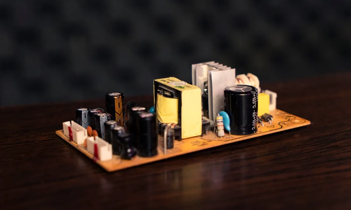
Inside the Assembly
Map Every Interface in the Power Conversion System
Power electronics rarely have one interface. Device packages, modules, magnetics, busbars and control boards create different heat flux, voltage and mechanical requirements.
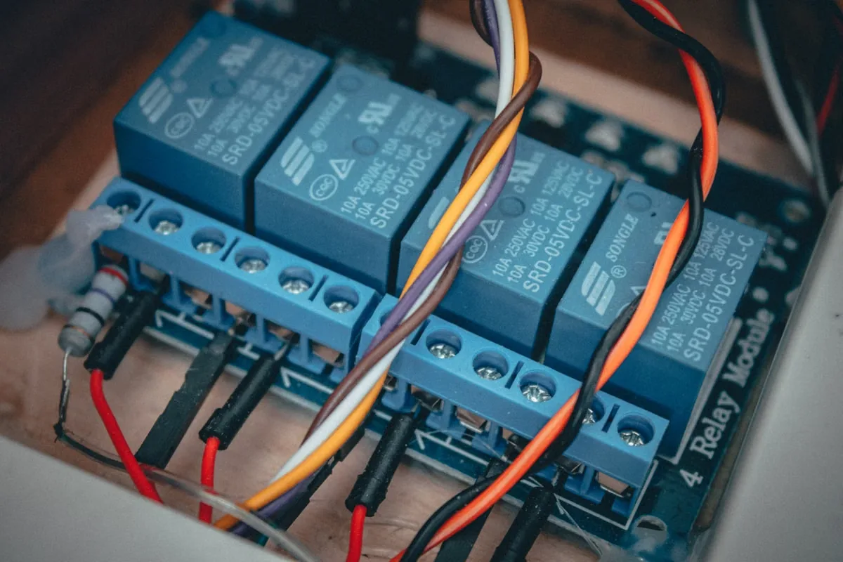
IGBT and MOSFET Modules to Heat Sink
Reduce case-to-sink resistance while maintaining electrical isolation, controlled mounting pressure and stable contact through repeated power cycles.
Read the IGBT Thermal Pad Guide →
MOSFETs, Drivers and PCB Hot Spots
Bridge component-height variation and move heat into a spreader or enclosure without overloading packages, solder joints or circuit boards.
See the MOSFET Selection Guide →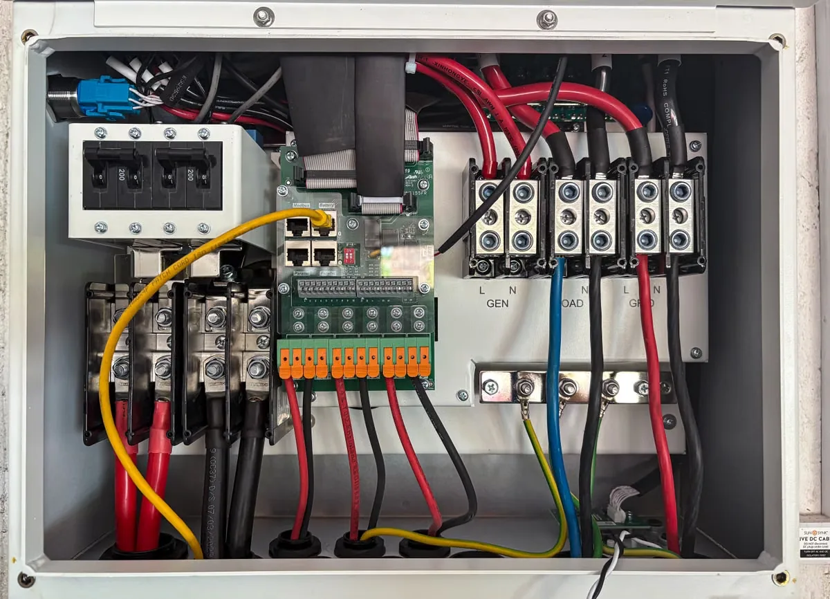
Inverters, Converters and Motor Drives
Coordinate module cooling with inductors, transformers, capacitors and sealed enclosures across high load, vibration and field-service conditions.
Explore Thermal Paste for Inverters →Material Families
Choose the Interface Function Before the Chemistry
Start with gap, flatness, heat flux, voltage, pressure and service conditions. Then compare the material format that can maintain the required interface over time.
Electrically Insulating Thermal Pads
Combine gap filling, dielectric isolation and controlled placement between devices, modules and metal cooling structures.
- Sheet, roll or die-cut format
- Defined thickness and hardness
- Compression-controlled contact
Low-Resistance Thermal Grease
Wet thin, flat and firmly clamped interfaces where a low bond line is more important than filling a large mechanical gap.
- Thin case-to-sink interface
- Low contact resistance
- Serviceable assembly
Phase Change Interface Materials
Soften at operating temperature to improve wetting while offering cleaner placement than conventional grease.
- Controlled pre-applied format
- Thin bond-line potential
- Production-friendly handling
Dispensable Gap Fillers
Conform around inductors, transformers, capacitors and uneven board assemblies with low mechanical stress.
- Variable and complex gaps
- Manual or automated dispense
- Soft cured interface
Thermally Conductive Adhesives
Create a thermal path and structural attachment where screws, clips or separate fixation are impractical.
- Bonding plus heat transfer
- 1K or 2K cure options
- Controlled modulus and strength
Potting and Encapsulation
Protect power boards and components against moisture, contamination, vibration and electrical exposure.
- Thermal and dielectric balance
- Selective or complete fill
- Cure and exotherm control
Format Comparison
Match the Material to the Real Power Interface
The best option is the one that reaches the required temperature, voltage margin and service life at final thickness and mounting pressure.
| Material Format | Best-Fit Interface | Primary Advantage | Design Watch Points |
|---|---|---|---|
| Thermal pad | Power module, MOSFET, driver board or uneven housing gap | Gap filling plus dielectric isolation | Thickness, hardness, compression and cut-edge quality |
| Thermal grease | Thin, flat, clamped module-to-heat-sink interface | Low bond line and excellent wetting | Pump-out, migration, application volume and maintenance |
| Phase change TIM | Flat device or module interface needing clean placement | Controlled handling and operating-temperature wetting | Activation temperature, pressure and cycling stability |
| Liquid gap filler | Magnetics, capacitors, PCB assemblies and complex enclosures | Conformance across variable component heights | Dispense control, cure, voids and rework |
| Thermal adhesive | Heat sink, spreader, sensor or component requiring fixation | Mechanical bond and heat path in one material | Cure, stress, strength and removal strategy |
| Potting compound | Power board, converter cavity and protected high-voltage electronics | Environmental and dielectric protection | Exotherm, stress, mass, voids and full cure |
Selection Workflow
Build the Power Interface Brief in Five Steps
A useful material brief connects junction losses and mechanical stack-up to measurable interface, insulation, production and reliability requirements.
Define the Heat Path
Identify device losses, switching profile, junction limit, case temperature and target cooling structure.
Measure the Interface
Record contact area, flatness, roughness, minimum and maximum gap, fastener pattern and torque.
Set Electrical Limits
Confirm working voltage, dielectric target, creepage, clearance and isolation architecture.
Choose the Process
Define pad placement, grease printing, dispensing, cure, inspection, cycle time and rework.
Validate Reliability
Test thermal impedance, insulation and contact stability through power cycling, vibration and aging.
Engineering Variables
What Should Be Specified Before Sampling?
Power material selection improves when the sample represents the actual heat flux, voltage, surface condition, pressure and cycling profile. Share a range when the mechanical design is not frozen.
The complete junction-to-coolant path—not one datasheet value—defines system performance.Device Losses and Temperature
Steady and transient power, switching frequency, junction limit, case temperature and cooling target.
Gap and Surface Condition
Bond-line range, flatness, roughness, parallelism, contact area, baseplate bow and tolerance stack-up.
Mounting Pressure
Fastener pattern, torque, clamp load, pressure distribution, package stress limit and thermal expansion.
Electrical Isolation
Working voltage, transient voltage, dielectric strength, insulation thickness, creepage and clearance.
Reliability Profile
Power cycling, thermal cycling, vibration, humidity, high-temperature aging and field service life.
Manufacturing Process
Placement or dispense method, application volume, cure, takt time, inspection and repair strategy.
Failure Prevention
Design Around the Risks That Appear After Assembly
Initial thermal performance can look acceptable while the interface still loses contact, insulation margin or process repeatability after cycling.
Excessive Bond-Line Thickness
A material that is too thick can add bulk resistance even when its advertised conductivity is high.
Review Pad Thickness Selection →Uneven Pressure or Package Stress
Fastener location, torque and pad hardness can create hot spots or overload ceramic packages and solder joints.
Understand Compression Effects →Insufficient Isolation Margin
Cut edges, pinholes, thickness variation and aging can reduce real assembly insulation below coupon expectations.
Read the Electrical Insulation Guide →Grease Pump-Out or Migration
Thermal expansion and power cycling can move grease away from the active interface and increase resistance.
Review Grease Service Life →Poor Contact Across Uneven Gaps
A thin-interface material cannot compensate for large height differences, warped boards or tilted heat sinks.
Compare Putty and Pad Formats →Potting Exotherm and Cure Stress
Large casting volumes can generate heat and shrinkage stress around boards, magnetics and power components.
Plan the Potting System →Power Platforms
Different Systems Create Different Interface Priorities
Topology, voltage, switching device, cooling method, load cycle and enclosure determine the best balance of impedance, insulation and manufacturability.

EV Inverters and Onboard Chargers
- High voltage and high heat flux
- Vibration and power cycling
- Compact liquid-cooled stack
Industrial Drives and Inverters
- Long operating life
- Rugged enclosure and vibration
- Serviceable interfaces

Power Supplies and DC/DC Converters
- Multiple component heights
- Magnetics and semiconductor cooling
- Compact forced-air systems
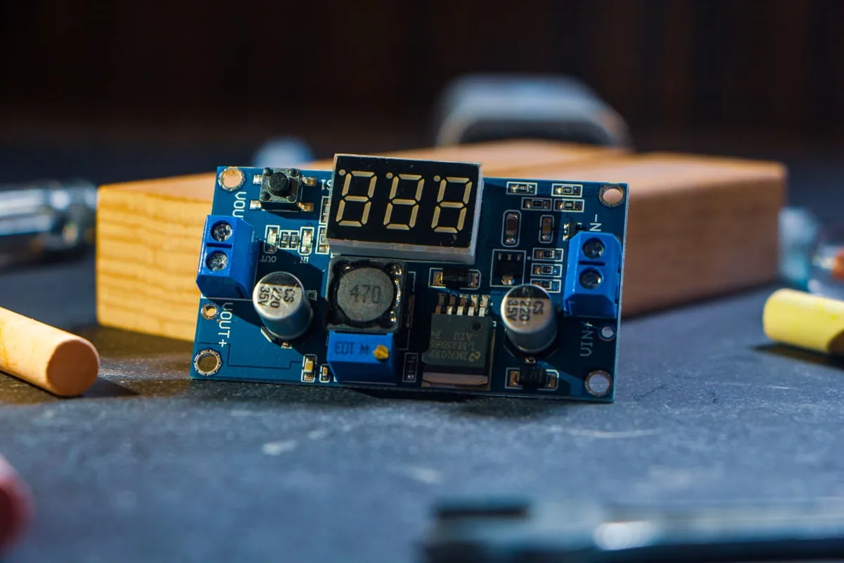
Drivers, Chargers and Control Modules
- Board-to-housing heat transfer
- Dielectric protection
- Automated volume assembly
Validation Plan
Test the Final Stack, Not Only the Material Coupon
Coupon data helps compare candidates. System testing confirms whether the interface maintains temperature, insulation and contact through real pressure and cycling conditions.
Review Common TIM Test Standards →Thermal Impedance
Measure case-to-sink or component-to-coolant performance at actual thickness, pressure and temperature.
Pressure Distribution
Confirm torque, clamp load, flatness and interface contact without package or PCB overstress.
Electrical Safety
Validate dielectric strength, insulation resistance and cut-edge integrity after assembly and aging.
Power Cycling
Track thermal resistance change through device heating, expansion and repeated operating cycles.
Environmental Aging
Evaluate high-temperature storage, humidity, vibration and application-specific chemical exposure.
Production Capability
Check pad placement, grease volume, dispense accuracy, cure window, inspection and rework.
From Prototype to Production
Material Performance Must Survive the Manufacturing Process
Haktak can support formulation and delivery format. Share mounting drawings, equipment constraints, annual volume, package size, placement method and reliability targets early.
Custom Formulation
Tune conductivity, viscosity, hardness, dielectric behavior, cure and temperature stability.
Die-Cut Conversion
Supply pads and films with holes, tabs, liners and placement-ready geometry.
Dispensing Support
Align grease, gap filler or adhesive packaging with bead, shot size, equipment and cycle time.
Prototype Samples
Compare formats and property ranges before final tooling, validation and production release.
Engineering Resources
Build a Stronger Power Electronics Material Specification
Use these guides to compare material formats, define interface geometry and prepare a practical validation plan.
How to Choose Thermal Pads for Power Electronics
Connect gap, pressure, insulation and reliability to pad thickness and hardness.
Read the Power Electronics Guide →Ceramic Sheets vs. Thermal Pads
Compare rigidity, insulation, conformability and manufacturing trade-offs for IGBT and MOSFET systems.
Compare Isolation Formats →Thermal Paste for High-Power Amplifiers
Review thin-interface wetting and stability in demanding clamped power assemblies.
Read the High-Power Guide →Thermal Resistance vs. Thermal Impedance
Understand how material, contact and test conditions affect reported interface performance.
Review Thermal Metrics →How Bond-Line Thickness Affects Performance
See why final thickness belongs in every case-to-sink material comparison.
Review Bond-Line Effects →Browse Haktak Material Products
Review available thermal and adhesive product families and individual grades.
Browse All Products →Frequently Asked Questions
Power Electronics Thermal Material FAQ
Final selection should be validated in the real module, heat sink, voltage and mounting stack.
Which thermal material is best for an IGBT module?
Thermal grease, phase change material and electrically insulating thermal pads are common options. The correct choice depends on flatness, bond-line thickness, mounting pressure, voltage isolation, pump-out risk and production handling.
Should I use thermal grease or a thermal pad for a power module?
Use grease for a thin, flat and firmly clamped interface where low contact resistance is the priority. Use a pad when the assembly needs gap filling, defined thickness, clean placement or additional dielectric isolation.
Is higher thermal conductivity always better for power electronics?
No. Final impedance also depends on thickness, pressure, wetting and contact resistance. A highly conductive material can underperform if it is too thick, too firm or unstable through cycling.
How is electrical isolation evaluated at the thermal interface?
Review working and transient voltage, dielectric strength, thickness, creepage, clearance and cut-edge geometry. Validation should include the assembled part after compression, cycling and environmental aging.
How can thermal grease pump-out be reduced?
Use controlled application volume, stable clamping, compatible viscosity and a formulation validated through the expected power-cycling range. Surface flatness and thermal expansion mismatch also affect migration.
What information does Haktak need for a recommendation?
Share the device type, losses, contact area, gap, surface condition, mounting pressure, voltage, temperature target, cycling profile, manufacturing method and expected volume.
Start With the Complete Power Stack
Send the Heat Load, Voltage, Gap and Mounting Process
Haktak can help compare thermal pads, grease, phase change materials, gap fillers, adhesives and potting systems for the complete power electronics assembly.