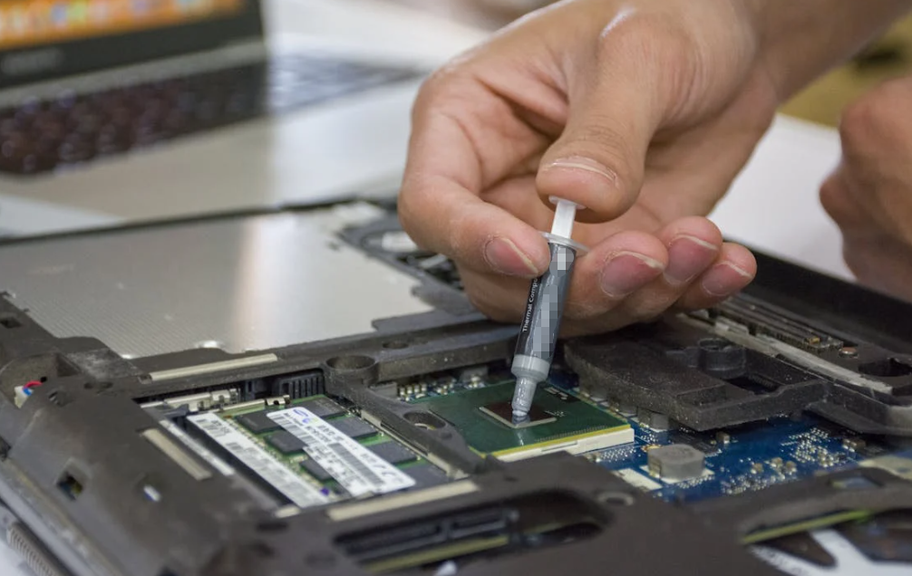
You open a power supply and find a thin, slightly rubbery sheet between a voltage regulator and its metal heat sink. The regulator is screwed down tight. The sheet looks almost too simple to matter, but take it away and you may get a hotter IC, an electrical short, or both.
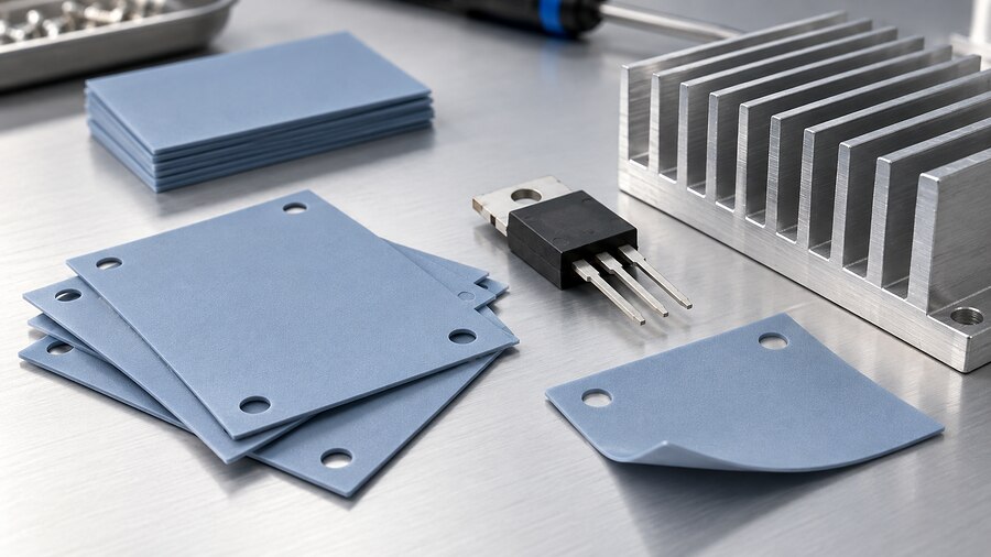
That sheet is often called a sil pad. It is a preformed thermal interface placed between the outside of an electronic package and a cooling surface. Its main job is to help heat cross the joint. An electrically insulating grade also keeps a live package surface from touching the heat sink. Those are two separate requirements, and the exact material has to meet both when both are needed.
There is a naming wrinkle. BERGQUIST SIL PAD® is a product family from Henkel; “sil pad” is also used informally for similar silicone-based thermal insulator sheets. So when a repair note says “replace the sil pad,” don’t assume every sheet in the catalog has the same electrical rating. The interesting question is what this IC, this mounting point, and this heat sink need.
What is a sil pad in an IC assembly, exactly?
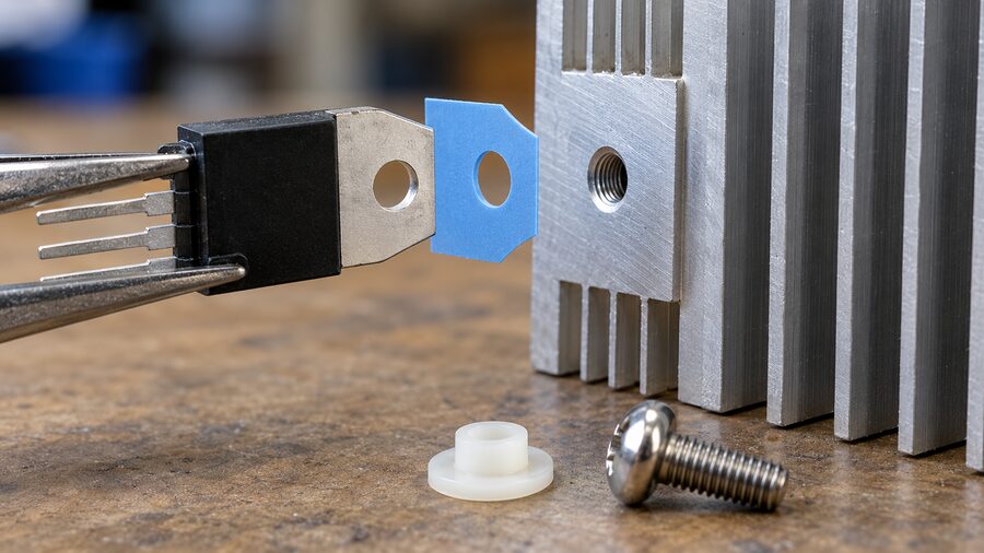
Picture the stack from the side. There is an IC package, a thin sheet and a metal heat sink. The sheet touches the package case or mounting tab, not the bare silicon circuit inside it. Heat generated at the semiconductor junction travels through the package, crosses the sheet and enters the sink.
Why put anything between the two? Surfaces that look flat have tiny peaks and valleys. Press the package against bare metal and much of the apparent contact area still contains air. A suitable pad compresses and fills part of that roughness. Heat can then cross more of the interface. If the pad is electrically insulating and properly installed, it can also block a current path between the package and sink.
The name is easy to muddle with two other kinds of “pad” used around chips:
| Term you may see | Where it is | What it does |
|---|---|---|
| Separate sil pad or thermal insulator sheet | Between a package or board and a heat sink, housing or rail | Improves heat contact; a qualified grade may provide electrical isolation |
| Exposed thermal pad on an IC package | Built into the underside of packages such as some QFNs | Often soldered to a specified PCB land; electrical connection depends on the device |
| Thermal land and vias on a PCB | Copper pads and plated holes in the board | Carry heat from a package into copper layers or another cooling path |
Do not slide a silicone sheet under a QFN exposed pad in place of its specified solder joint. Check the IC manufacturer’s land-pattern instructions. And do not press an ordinary cut sheet against a bare die unless the package design explicitly calls for that interface. In most of this article, “sil pad” means the separate sheet outside the package.
For the name and the range of branded constructions, see Henkel’s BERGQUIST SIL PAD® material family. HAKTAK’s own equivalent category should be specified by its actual construction and test data, not by a competitor’s trademark.
Follow the heat from the IC to the room
The pad is only one stop on a longer trip. For a simple heat-sink-mounted power device, the route looks like this:
Junction → package case → thermal interface → heat sink → surrounding air
Engineers often call the first thermal resistance junction-to-case (RθJC). The pad and its two contacts contribute to case-to-sink (RθCS). The sink and its environment supply sink-to-ambient (RθSA). For an idealized, mostly single-path arrangement, an early estimate is:
Tj ≈ Ta + P × (RθJC + RθCS + RθSA)
Here Tj is junction temperature, Ta is ambient temperature and P is the power dissipated as heat in watts. Resistances are in K/W or °C/W for temperature differences. This estimate assumes a consistent heat path and steady conditions. A PCB may also carry heat away, so real assemblies can need a more detailed model.
Say a regulator dissipates 8 W. If the assembled interface resistance rises by 0.5 K/W, and everything else stays the same, the simple model predicts about 4°C more junction-to-ambient rise. Those are illustrative numbers, not a test result for a particular product. It shows why a small sheet can matter.
The reverse is important too. If the heat sink has weak airflow and already dominates the thermal budget, changing the pad alone may yield little improvement. Likewise, buying a pad with a bigger W/m·K number will not solve an interface that barely touches one side. Well, the contact is the whole point.
For MOSFET-specific examples, including package style and heat budget, HAKTAK’s MOSFET thermal pad selection guide goes further into that assembled path.
When does a sil pad electrically isolate an IC?
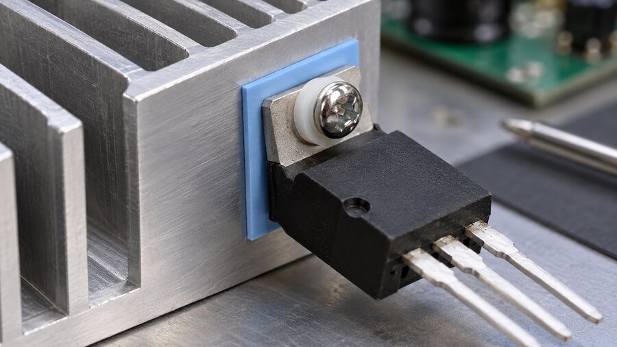
Start by checking the package drawing and the circuit. Some TO-220 or TO-247 style devices have a metal tab connected to a live electrical node. A power MOSFET tab is often tied to its drain, for example, but the exact device data sheet decides. Regulators and rectifiers have their own tab connections. If that tab touches a grounded, touchable or shared metal heat sink, the result can be a short or an unsafe enclosure.
In that situation, an electrically insulating sheet may provide a heat path while separating the tab from the sink. But a pad is not automatically required for every IC. A fully insulated package may already provide the needed barrier. In another design, the entire sink is intentionally isolated. On a PCB-mounted QFN, the main thermal path may run into copper and vias instead of through a separate sheet. Draw the actual electrical and thermal boundaries before ordering material.
HAKTAK’s guide to electrically insulating thermal pads is useful when a package, chassis and heat sink sit at different potentials. It frames isolation as a property of the assembled joint, not a reassuring word on a product label.
The sheet does not insulate the mounting screw
Here’s a mistake that looks obvious only after it has happened. The pad sits neatly under the metal tab. The mounting screw passes through the tab and touches the heat sink. Current can now go around the sheet. On a design that needs isolation, an appropriate shoulder bushing or other specified insulating hardware may also be required.
The pad itself must cover the intended metal contact area. Watch for burrs, sharp edges, washer impressions and die-cut holes that leave too little material. Excessive clamping can cut through some constructions. Too little clamping leaves air in the joint. The safe answer depends on the package and mounting-hardware instructions, not an internet torque value borrowed from another transistor.
Electrical breakdown voltage is measured on a specimen under stated conditions. It is not a promise that the same voltage is safe forever in a humid, vibrating, bolted assembly. The ASTM D149-25 method covers dielectric breakdown voltage and dielectric strength of solid insulating materials at commercial power frequencies. Use it to understand how a material was tested. Then qualify the finished mounting arrangement against the actual product’s electrical requirements. Check creepage and clearance around the sheet as well as puncture through it.
What is inside a sil pad?
Many pads combine a silicone elastomer with thermally conductive filler. Fillers such as alumina or boron nitride can move heat while allowing a formulation to remain electrically insulating. A reinforcement layer may improve handling and resistance to tearing or cut-through. A carrier film can help a thin part survive cutting and assembly.
“Silicone” is the polymer family used in many of these pads; it is not the silicon chip inside the IC. Small wording difference, big materials difference.
And the broad label “thermal pad” tells you almost nothing about electrical isolation. A graphite or carbon-rich sheet may be an excellent heat spreader and still conduct electricity. Some silicone-based products are designed for different electrical behaviors, too. Ask for the exact grade’s dielectric data whenever the sheet is part of the insulation system.
| Construction | Why it may fit an IC assembly | What needs closer checking |
|---|---|---|
| Soft, ceramic-filled silicone pad | Conforms to imperfect surfaces and bridges a defined gap | Installed thickness, force, dielectric test and long-term compression |
| Fiberglass-reinforced silicone sheet | Thin controlled placement and improved handling | Contact under available pressure and resistance to edge damage |
| Polyimide-supported thermal sheet | Thin carrier with useful mechanical and dielectric properties | Performance of the whole laminate, including any coating or adhesive |
| Silicone-free thermal pad | Option where silicone contamination is a documented concern | Exact insulation rating, temperature range and pressure response |
| Mica or ceramic insulator | Rigid electrical barrier for suitable flat, clamped joints | Fragility, flatness and any specified interface compound on each face |
| Graphite or carbon-rich thermal sheet | Often used for heat spreading | May be electrically conductive; do not assume isolation |
For a compliant sheet where insulation and compression both matter, compare HAKTAK’s silicone thermal pads against the actual gap and load. A thinner, tougher die-cut barrier may instead lead you to a reinforced thermal silicone cloth construction. Those links point to material categories, not a promise that every available grade meets the same voltage or heat target.
If an optical surface, contact or downstream coating process is genuinely sensitive to silicone, silicone-free thermal pads are another category to investigate. The replacement still needs its own thermal and electrical qualification. Switching polymer chemistry does not magically solve the mounting problem.
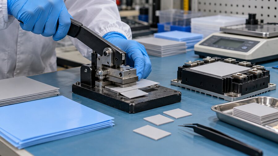
Sil pad, thermal grease, mica or thick gap filler?
These materials do different jobs in the same general neighborhood. Picking between them by touch or color is like choosing a gasket because it happens to be blue.
| Option | What it does well | Isolation and assembly caution |
|---|---|---|
| Thin electrically insulating sheet | Clean, repeatable placement at a flat, clamped interface | Verify the exact dielectric rating and complete mounting path |
| Thermal grease | Very thin contact layer on suitable flat joints | Grease alone should not be treated as a dependable isolation barrier |
| Mica or ceramic with specified TIM | Rigid barrier in a controlled mounting stack | May need careful treatment of both contact faces and a compatible clamp |
| Soft, thicker gap filler pad | Bridges a larger or variable board-to-housing gap | Extra thickness and force can hurt a tightly mounted power device |
| Phase-change film | Can improve contact after reaching its working condition | Check electrical behavior, mounting method and heat-cycle performance |
One more distinction: a thermal pad is not automatically an adhesive. A slightly tacky surface can help placement, but the heat sink normally needs its designed clip, screw or bracket. If a structural bond is needed, specify a bonding system built for that job.
Can grease be added to both sides of a sil pad? Sometimes a manufacturer’s instructions call for a compound with a particular insulator. Other pads are meant to work cleanly without it. Extra grease can make assembly messy and may not improve an already conformable interface. Follow the specific grade’s application guidance and verify the result in the assembly. A generic “always add paste” rule is no help here.

Choose and install the pad around the actual IC
Let’s make this concrete. Suppose a power-supply board has two TO-220 devices mounted on one aluminum rail. Their tabs are at different potentials. The drawing calls for electrical separation, and the rail gets warm in operation. The selection process should look roughly like this:
- Identify the parts. Read each package and device data sheet. Mark the metal tab’s electrical node and the heat path from junction to case. Do not assume two packages with the same outline have the same tab connection.
- Set the isolation boundary. Decide whether tab-to-rail insulation is needed for each device. Include the fastener, washer or clip, the edge of the pad and the rail itself. The little shoulder washer can be as important as the big pink rectangle.
- Measure the real joint. Check package flatness, rail finish, available contact area, stack height and mounting-force limits. For a housing-spanning pad, include minimum and maximum gaps; HAKTAK’s guide to thermal pad thickness selection provides a deeper tolerance workflow. For a closely clamped transistor tab, make sure you do not substitute a thick, soft enclosure pad merely because both products are called thermal pads.
- Shortlist qualified constructions. Ask for the supplied and installed thicknesses, through-plane thermal properties, dielectric data, cut-through behavior and recommended mounting conditions. A more conductive grade can be firmer. If the available clip force is low, the “better” W/m·K figure may fail to buy you good contact.
- Prepare the parts. Inspect the rail for burrs and sharp machining marks. Clean the mating faces as specified. Confirm a die-cut sheet covers the intended tab area without fouling the mounting hardware. Remove both release liners if the product has them; a forgotten clear film can be surprisingly hard to spot.
- Mount with the specified hardware. Center the pad, fit the correct insulating bushing if required and tighten or clip the device according to its mounting instructions. Do not guess a torque from a different IC. The pad should seat without folding, sliding or being pinched at the hole.
- Test the assembled unit. Measure device temperature under the relevant load and ambient conditions. Perform the electrical withstand or isolation checks appropriate to the product. Where the application demands it, repeat after humidity exposure, vibration or thermal cycling.
For a simple analogy, the pad acts a bit like a soft gasket: it helps two imperfect faces meet. But it isn’t the entire gasket system if the bolt gives electricity another route around it. Both heat transfer and insulation depend on the finished joint.

Where are IC sil pads useful in practice?
In an industrial motor drive, a power MOSFET or rectifier may be clamped to a shared metal sink. A qualified insulating sheet can help keep a live tab away from that metal while allowing heat out. The same design has to control screw isolation and the sink’s final temperature.
In a power supply or LED driver, a voltage regulator may run close to its thermal limit inside a small enclosure. A thin, reinforced interface can make assembly cleaner, provided the tab potential, mounting pressure and heat-sink airflow are known. Changing the sheet won’t compensate for a sealed box that has nowhere to dump the heat.
In telecom, EV auxiliary and other power electronics, board-to-housing distances can vary more than a screw-mounted tab interface. A softer gap pad may be the better shape for that job. It might still need dielectric performance, but you should not judge it by the same thickness or pressure expectations as a thin transistor insulator.
A processor or high-performance chip can use a completely different cooling stack: package lid, paste or phase-change material, heat spreader and mechanical retention. The fact that it is an IC doesn’t automatically mean a separate sil pad should go under its lid. The package and thermal design decide.

If the IC still overheats, check the joint before buying a higher W/m·K pad
The headline conductivity number is a material property, usually in W/m·K. What you really care about is how much temperature rise the installed interface adds. Pad thickness, pressure and contact at both faces change that result. The ASTM D5470-17(2024) thermal transmission method measures thermal impedance and discusses apparent conductivity for these materials. When comparing two sheets, ask whether their impedance figures use comparable thickness, temperature, surface condition and pressure. HAKTAK also explains thermal conductivity versus thermal impedance in more detail.
| Symptom | First things to inspect | What a useful test shows |
|---|---|---|
| Device hotter after a pad swap | Compressed thickness, hardness, surface contact | Whether the new sheet actually seats at the available force |
| Hot spot at one corner | Tab flatness, sink warp, pad alignment | A contact imprint or measured temperature map |
| Good contact, but whole sink is hot | Airflow, fin orientation, enclosure temperature | Whether sink-to-air cooling is the bottleneck |
| Intermittent electrical fault | Screw bushing, pad coverage, burrs, cut-through | Where the assembled insulation path fails |
| Temperature drifts after months | Clamp relaxation, movement, aging, contamination | Results before and after relevant stress tests |
Suppose Pad A is thin and rated at 2 W/m·K, while Pad B is twice as thick and rated at 3 W/m·K. Ignoring contact and holding area constant, their bulk resistances scale as thickness divided by k: A is proportional to 1/2; B to 2/3. B’s bigger conductivity number does not win that simplified comparison. But if A is too firm to contact a warped rail, the assembled result may reverse. That’s why the installed impedance and device-temperature check earn their place.
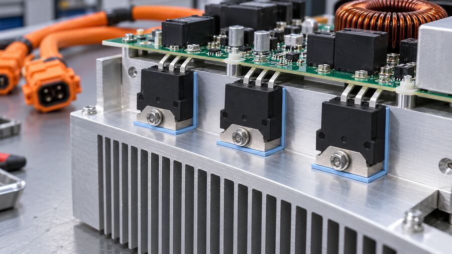
What data and standards belong on the supplier brief?
Ask for the exact product grade and construction, including any fiberglass, polyimide film, adhesive backing and cut geometry. Request supplied thickness tolerance and, where applicable, compressed thickness at the real mounting load. For thermal comparison, record the test method, pressure and sample thickness behind the reported impedance. For electrical comparison, record the tested specimen thickness, dielectric method, electrodes, conditioning and voltage type.
ASTM D5470 is relevant to thermal transmission. ASTM D149 covers AC dielectric breakdown under specified conditions. UL 94 may appear on a sheet’s data sheet, but it classifies flammability behavior; it does not prove the mounted IC is electrically isolated. Component-maker mounting notes, such as those from onsemi, can guide clip or screw installation for their own package families. Check the exact part drawing before setting hardware or force.
Finally, look at the sector-specific environment. A lab supply, an outdoor telecom converter and an EV control module do not see the same humidity, vibration or cycling. Qualification should reflect the actual use case. HAKTAK’s material selection and testing page is a place to organize that supplier discussion.
Conclusion
A sil pad in an IC assembly is a separate thermal interface sheet placed between the outside of a package and a cooling surface. In the right grade and mounting stack, it helps move heat while keeping a live surface electrically apart from the heat sink. The sheet alone does not answer every question: the package, screw, contact pressure, pad thickness and downstream cooling all count. Identify the electrical boundary first, then test the installed heat path. Simple, in theory. Much more reliable in practice.
FAQs
Is a sil pad the same thing as a silicone thermal pad?
People use the names loosely. SIL PAD® is Henkel’s product-family name. A silicone thermal pad is a broader material category, and not every such pad has the same reinforcement or dielectric rating. Check the exact construction rather than the nickname.
Does every IC need an insulating pad against its heat sink?
No. It depends on the package, tab potential, cooling path and heat-sink voltage. Some packages are internally insulated; some use PCB copper and vias for cooling. An added sheet may increase thermal resistance without providing a needed benefit.
Is the exposed thermal pad under a QFN the same as a separate sil pad?
No. The QFN feature is part of the package and is commonly soldered to a specified PCB land. A separate sil pad is installed outside a package at a mechanical cooling interface. Follow the part maker’s footprint and electrical instructions.
Can I use thermal grease instead of a sil pad on a live tab?
Do not assume grease provides the electrical isolation required between a live tab and a metal heat sink. If insulation is required, use an appropriately qualified insulating construction and mounting hardware, or another approved system design.
Do I need a shoulder washer with a TO-220 sil pad?
If an electrically live mounting tab is fastened to a sink that must stay isolated, the screw path may need an insulating bushing. The specific package, screw and mounting drawing determine the hardware. The sheet only covers the broad face.
Should I put thermal paste on both sides of a sil pad?
Only if the specific insulator supplier and mounting design call for it. Some preformed pads are intended to be installed clean and grease-free. Test contact and temperature instead of adding paste out of habit.
How thick should a sil pad be for a power IC?
There is no one thickness for every IC. Choose from the real gap, required electrical barrier, pressure, package flatness and tested thermal impedance. For a clamped tab, a thin reinforced sheet and a thick enclosure gap pad solve different jobs.
Can a graphite thermal pad electrically isolate an IC?
Many graphite-based products are electrically conductive. Never rely on graphite for electrical isolation without explicit grade-level evidence and assembly qualification. High thermal conductivity does not tell you its electrical behavior.
Which number predicts IC temperature better: W/m·K or thermal impedance?
Thermal impedance measured at relevant thickness and pressure is closer to the real interface than bulk conductivity alone. Even then, junction temperature also depends on package resistance, power loss, heat-sink design and ambient conditions.
Can I reuse a sil pad after removing the heat sink?
Do not assume so. A removed sheet may stretch, tear, collect debris, lose position or change how it contacts the surfaces. Follow the specific product’s rework guidance; if the pad is damaged or insulation is critical, replace it and check the assembled joint again.