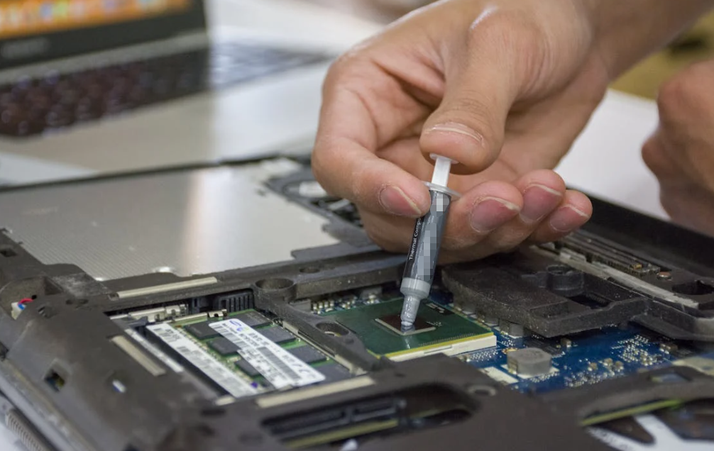
A custom thermal pad should not begin with a color, a thickness, or a big W/mK number. It should begin with the product.
Where is the heat generated? Where can it go? What gap must be filled after every tolerance is included? How much force can the component and PCB tolerate? Does the interface also need electrical insulation? What happens after five years of heat, cold, vibration, and pressure?
Those questions are less exciting than browsing a material table. They are also the questions that stop a thermal pad from becoming an expensive blue rectangle that does very little.
The practical answer is straightforward: a custom thermal pad is designed by converting system requirements into a controlled material, thickness, compression window, shape, layer construction, validation plan, and production format. Thermal conductivity matters. The complete interface matters more.
What Makes a Thermal Pad “Custom” in 2026?
A custom thermal pad is a pre-formed thermal interface material developed or converted for a specific assembly. Customization can be as simple as cutting a standard pad into a unique outline. It can also include a special material formulation, thickness, hardness, conductivity, dielectric target, reinforcement, tack level, adhesive layer, release liner, color, flame rating, packaging, or automated-placement format.
Common custom options include:
- non-standard thickness;
- softer or firmer compression response;
- higher or lower thermal conductivity;
- silicone-free or fluorosilicone chemistry;
- fiberglass or film reinforcement;
- one-sided or selective PSA;
- custom die-cut holes, slots, tabs, and keep-outs;
- kiss-cut arrays or roll-fed parts;
- permanent insulation film;
- part marking, liner printing, and lot traceability.
HakTak’s guide to thermal interface materials provides the wider context. Thermal pads are one TIM family among grease, phase-change materials, graphite, putty, gels, liquid gap fillers, and thermally conductive adhesives.
Custom Does Not Always Mean a New Chemical Formula
Many successful projects use an existing material grade with a custom thickness, shape, liner, or packaging format. That is usually faster and easier to qualify than developing a new formulation.
A new material formula makes sense when standard products cannot meet a critical requirement, such as unusually low compression force, a specific conductivity-hardness balance, restricted siloxane content, fuel resistance, unique dielectric behavior, or a special processing format.
The more chemistry changes, the more validation and change control are needed. No surprise there.
Step 1: Define the Heat Source and Cooling Destination
Every custom thermal pad needs a defined heat path:
heat source -> thermal pad -> heat spreader, housing, heat sink, or cold plate -> ambient or coolant
The design team should record:
- component or module name;
- power dissipation under relevant duty cycles;
- maximum allowed case or junction temperature;
- available contact area;
- heat sink or housing material;
- ambient or coolant temperature;
- airflow or coolant flow condition;
- thermal resistance budget allocated to the interface.
Power alone is not enough. A 20 W component spread across a large metal base behaves differently from a 20 W hot spot inside a tiny package. Heat flux, spreading resistance, and contact area affect the interface requirement.
Map Useful Contact Area, Not Just Component Size
The thermal pad should cover the area where both surfaces can make useful contact. Material extending over empty space does not create extra cooling. It may still increase assembly force or interfere with nearby parts.
The simplified material resistance is:
R = t / (k x A)
where t is compressed thickness, k is thermal conductivity, and A is effective contact area. Real performance also includes contact resistance at both surfaces, spreading through the housing, and the rest of the cooling system.
This is why the pad cannot be designed in isolation from the housing and fastening system.
Step 2: Measure the Real Gap and Build a Tolerance Stack
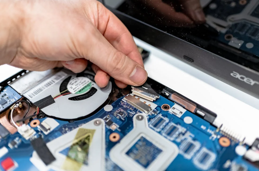
The nominal CAD gap is only the middle of the story. Production assemblies include:
- component height tolerance;
- solder joint thickness;
- PCB thickness and warpage;
- housing flatness;
- heat sink machining or casting tolerance;
- gasket compression;
- screw torque and clamp variation;
- adhesive thickness;
- thermal expansion across operating temperature.
The design needs three values: minimum gap, nominal gap, and maximum gap. HakTak’s thermal pad thickness selection guide explains how those values define the usable compression window.
A Simple Gap Example
Assume an electronics module has:
- minimum gap: 0.85 mm;
- nominal gap: 1.00 mm;
- maximum gap: 1.25 mm.
A 1.0 mm pad cannot reliably contact both surfaces at the maximum gap. A 1.5 mm pad would compress by roughly 43% at the minimum gap, 33% at nominal, and 17% at maximum. Whether that works depends on the pad’s force-deflection curve, recommended compression range, and the assembly force limit.
| Gap condition | Gap | Compression of a 1.5 mm pad | Main question |
| Minimum | 0.85 mm | About 43% | Is force, stress, or extrusion too high? |
| Nominal | 1.00 mm | About 33% | Does temperature meet the target? |
| Maximum | 1.25 mm | About 17% | Is contact pressure still sufficient? |
The same pad can be over-compressed in one unit and under-compressed in another. Nominal-only design misses that risk.
Step 3: Set the Mechanical Force Limit
Thermal pads need compression to conform to surface roughness and remove air pockets. Compression also creates load.
Total force is approximately:
force = pressure x pad area
That simple multiplication catches many bad designs. A soft pad over a small IC may create little concern. The same pressure across a large battery module can produce a very large total force.
The force limit should consider:
- PCB strain;
- solder-joint stress;
- ceramic capacitor cracking;
- package and die fragility;
- battery cell loading;
- housing deflection;
- fastener capacity;
- long-term creep and compression set.
HakTak’s explanation of thermal pad compression ratio shows why a percentage alone is not enough. Hardness, area, thickness, temperature, and viscoelastic behavior determine the actual load.
Hardness Is Not a Complete Force Specification
Shore 00 or Shore OO hardness is useful for comparing materials, but it does not replace a compression-deflection curve. Two pads with similar hardness can produce different force because their fillers, reinforcement, thickness, and polymer network differ.
Request pressure-versus-deflection data at the candidate thickness. Then calculate total force across the real pad area. For fragile assemblies, strain gauges or board-level modeling may be justified during prototype testing.
Step 4: Choose the Right Thermal Pad Material Family
The best material family depends on heat flow, gap, pressure, electrical needs, cleanliness, environment, and manufacturing.
| Material family | Best fit | Main advantage | Main tradeoff |
| Silicone gap pad | General electronics and uneven gaps | Soft, insulating, mature, easy to customize | Siloxane or bleed restrictions in sensitive systems |
| Silicone-free pad | Optical, relay, and contact-sensitive electronics | Reduces silicone-contamination concern | Different aging, tack, softness, and temperature behavior |
| Fluorosilicone pad | Oil, fuel, or chemical-exposed modules | Better resistance to many aggressive fluids | Higher cost and application-specific compatibility testing |
| Reinforced silicone insulator | Flat power devices and handling-critical parts | Puncture resistance and dimensional stability | Lower conformity than very soft pads |
| Graphite sheet | Thin devices needing lateral heat spreading | High in-plane spreading and low profile | Often electrically conductive and anisotropic |
| Phase-change TIM | Thin, flat, clamped interfaces | Low bond line after activation | Activation, pump-out, and rework considerations |
| Thermal putty | Complex multi-height components | Low-force conformity and flexible dispensing | Process control and rework considerations |
| Liquid gap filler | Large or irregular production gaps | Automated dispensing and low stress | Dispense, cure, inspection, and equipment requirements |
Custom Silicone Thermal Pads
Silicone pads remain a practical default for many electronics products. They can combine ceramic fillers, electrical insulation, softness, and a wide range of thicknesses. HakTak’s silicone thermal pad page outlines available sheet, roll, die-cut, hardness, tack, and thickness options.
Still, “silicone pad” is not one fixed material. Formulations differ in low-molecular siloxanes, oil bleed, volatile loss, tear strength, compression set, flame behavior, and surface tack.
Custom Fluorosilicone Thermal Pads
For modules exposed to fuel, oil, coolant, solvent vapor, or under-hood contamination, fluorosilicone may be worth evaluating. HakTak’s fluorosilicone thermal pad information lists the exposure data needed for sample selection.
Chemical-resistance charts are only screening tools. The actual fluid, concentration, temperature, duration, compression, and acceptable swelling limit should be tested.
Graphite Heat Spreaders
Graphite works differently from a soft gap pad. It is often strongest for lateral, or in-plane, heat spreading. It may need insulation film, adhesive, edge protection, or a compliant TIM beneath it.
HakTak’s graphite thermal pad guide explains why heat direction and electrical behavior should be defined before selecting thickness or shape.
Step 5: Compare Thermal Impedance, Not Only W/mK

Thermal conductivity is a bulk material property. Thermal impedance describes heat-flow resistance through an interface under defined thickness, pressure, temperature, and contact conditions. Device temperature is the system result.
A high-W/mK pad can perform poorly if it is too thick, too hard, or weakly compressed. A moderate-conductivity pad can perform better when it reaches a thinner bond line and makes fuller contact.
For example, ignoring contact resistance and using equal area:
- 6 W/mK at 1.5 mm gives a simplified
t/kterm of 0.25; - 3 W/mK at 0.6 mm gives a simplified
t/kterm of 0.20.
The lower-conductivity pad can have lower bulk resistance in this example. It is not a universal result. It is a reminder that thickness and contact cannot be separated from conductivity.
HakTak’s article on why high W/mK does not always mean better cooling explores this trap in more detail.
The current ASTM D5470 standard covers steady-state thermal impedance measurement and calculation of apparent thermal conductivity for TIMs. Supplier data should identify test pressure, specimen thickness, temperature, surface condition, and whether the result is typical or guaranteed.
Step 6: Define Electrical Insulation Requirements
Many thermal pads transfer heat and isolate electricity at the same time. That combination is useful, but the insulation system must be designed as a system.
Important inputs include:
- working voltage and transient voltage;
- AC, DC, and switching conditions;
- required breakdown voltage or dielectric strength;
- minimum compressed thickness;
- creepage and clearance around cut edges;
- volume resistivity;
- humidity and contamination level;
- altitude where relevant;
- proof-test or hipot requirements;
- aging before electrical retest.
ASTM D149 covers dielectric breakdown voltage and dielectric strength testing for solid electrical insulating materials at commercial power frequencies. A coupon result is useful, but the final product includes holes, cut edges, burrs, pressure, humidity, and possible contamination.
Thicker Is Not Automatically Safer
Increasing pad thickness may improve through-thickness electrical margin, but it also raises thermal resistance and can increase mechanical force. Over-compression can reduce the final insulation thickness. Cutouts can shorten the path around the material.
Electrical, thermal, and mechanical requirements therefore need one shared design review. Passing each calculation separately is not enough when the solutions conflict.
HakTak’s guide to electrically insulating thermal pads provides additional selection checks for power electronics and grounded housings.
Step 7: Design the Custom Thermal Pad Shape
Once material, thickness, and compression are credible, the XY geometry can be finalized.
A custom outline may need to:
- cover the functional thermal area;
- clear screws, bosses, connectors, and test points;
- maintain electrical edge distance;
- avoid vents, seals, and moving parts;
- provide orientation and anti-rotation features;
- support manual or automated placement;
- fit efficient material nesting;
- survive cutting and liner removal.
Use Radii and Remove Nonfunctional Detail
Sharp internal corners can become tear points. Narrow bridges can stretch during waste removal or placement. Tiny holes may recover after cutting and become smaller than expected.
Use rounded corners where possible. Widen fragile necks. Enlarge hardware clearances according to the full tolerance stack. Remove decorative geometry that does not improve heat transfer, clearance, orientation, or handling.
Detailed geometry should be reviewed directly with the converter before tooling is approved. Material thickness, softness, liner support, annual volume, and cutting process all affect practical feature limits.
Decide Whether One Large Pad or Several Small Pads Work Better
One large pad reduces part count and shifting risk. Several smaller pads can reduce material use, isolate force over individual components, and avoid bridging low components or empty space.
The right choice depends on:
- component-height variation;
- housing flatness;
- available pressure;
- placement accuracy;
- thermal spreading path;
- rework needs;
- die-cut yield;
- assembly time.
Connecting every thermal zone with a thin web may look tidy in CAD, but that web can tear or transmit unwanted force. Sometimes two simple pieces are the more robust design.
Step 8: Choose Adhesive, Tack, Liner, and Delivery Format
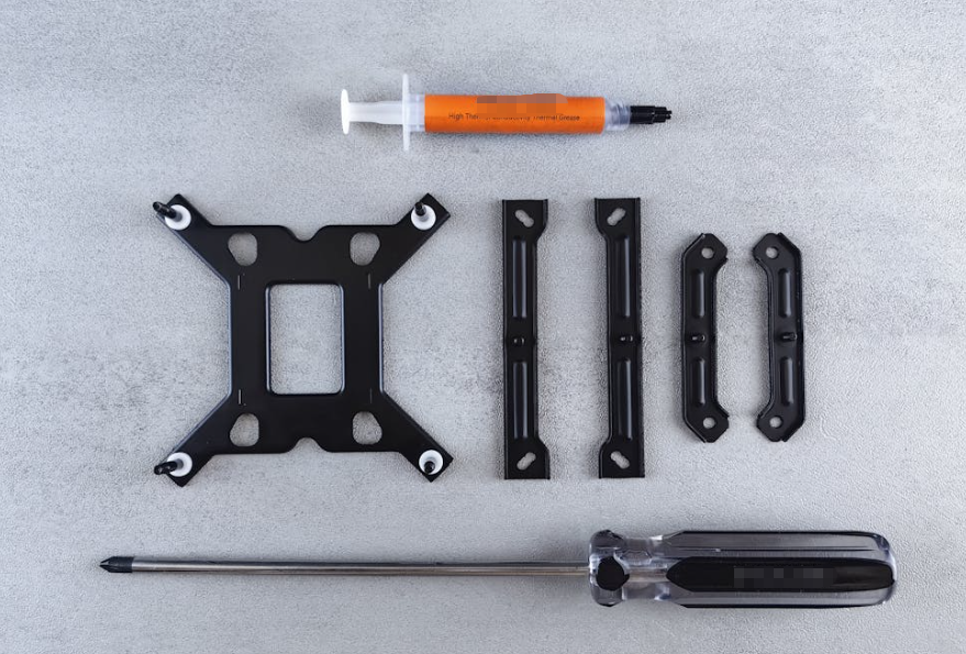
The thermal pad must reach the interface in good condition. Handling features are not an afterthought.
Natural Tack Versus Added PSA
Many silicone pads have enough natural tack for placement before the housing is closed. Added pressure-sensitive adhesive can hold the pad on a vertical surface or through intermediate shipping.
PSA also adds:
- thickness and thermal resistance;
- stiffness;
- another aging mechanism;
- possible residue;
- more difficult rework;
- lamination and registration tolerance.
Selective PSA may be better than full-area adhesive. A small attachment zone can hold the pad while keeping the primary thermal path free from an extra layer.
Release Liners and Pull Tabs
Release liners support soft material during cutting, keep surfaces clean, and control part presentation. A pull tab gives operators somewhere to grip without touching the thermal surface.
Define:
- which liner is removed first;
- which films are temporary or permanent;
- peel direction;
- liner overhang or split;
- release-force expectations;
- color and marking;
- compatibility with gloves or vacuum pickup.
A permanent reinforcement film should never be confused with a disposable liner. Color coding helps, but the drawing and work instruction must state the layer function clearly.
Pieces, Sheets, Arrays, or Rolls
| Delivery format | Best fit | Main benefit | Main risk |
| Individual pieces | Service kits and low volume | Easy counting and kitting | Loose-part handling and orientation |
| Kiss-cut sheets | Manual assembly and moderate volume | Organized placement and simple peel | Sheet curl and release consistency |
| Multi-part kits | Products using several pad shapes | Error-proofed assembly sequence | Kitting complexity and mixed-part control |
| Continuous rolls | Automated high-volume placement | Stable pitch and machine feeding | Web, splice, winding, and pickup requirements |
For rolls, specify pitch, web width, core size, maximum diameter, winding direction, part orientation, splice rules, and label position. A good part in the wrong winding direction can still stop a line.
Step 9: Match the Design to the Product Application
Different industries change the priority order.
| Application | Typical custom pad location | Primary design priorities |
| EV battery systems | Cells or modules to cooling plate, BMS to housing | Large-area force, insulation, thermal cycling, traceability |
| Automotive ECUs | Processor, MOSFET, or power board to cast housing | Vibration, gap tolerance, chemicals, dielectric aging |
| AI servers and GPUs | Memory, VRM, retimers, controllers to cold plate or lid | Low impedance, repeatability, serviceability, high power density |
| Power electronics | MOSFETs, IGBTs, SiC devices, magnetics | Insulation, pressure, flatness, cycling |
| LED lighting | LED boards and drivers to aluminum heat sink | Thin bond line, clean placement, optical compatibility |
| Telecom and 5G | ASICs, RF modules, power stages to chassis | Long life, sealed housing, hot-spot control |
| Consumer electronics | Processor, battery, charging circuit, display | Thin profile, graphite spreading, automated placement |
| Industrial controls | Drives, converters, sensors, rugged modules | Vibration, humidity, variable housings, field life |
| Medical electronics | Imaging, sensors, power modules | Cleanliness, traceability, controlled materials |
Battery and EV Products
Large battery interfaces need uniform compression and careful force calculation. Cell swelling, tray flatness, coolant plate structure, and long-term compression set can matter more than a small increase in W/mK.
AI Servers and High-Power Electronics
High-power hardware often uses several TIM types in one assembly. A thin phase-change material may serve a flat processor interface, while soft custom pads bridge gaps over memory, VRMs, retimers, or power components.
The design should not force one material to solve every interface. The thermal architecture decides where pads make sense.
Uneven Multi-Height Boards
When many component heights vary across one board, a complex set of pad thicknesses can become hard to manage. HakTak’s thermal putty versus thermal pad comparison explains why putty may fit low-pressure, irregular geometry more naturally. A thermal conductive liquid gap filler can also simplify automated production for large variable gaps.
Step 10: Prototype the Complete Thermal Stack
Datasheets help screen materials. Prototypes reveal the assembly.
Early samples should use:
- the intended material grade and thickness;
- production-like die-cut geometry;
- real liners and adhesive;
- actual housing surfaces;
- representative fasteners and torque;
- worst-case gap samples where possible;
- realistic ambient, airflow, or coolant conditions.
Digital-cut samples can confirm fit before hard tooling. The thermal result should still be checked again with production-converted parts because liner, edge, adhesive, and dimension control can differ.
Measure More Than Temperature
A useful prototype review includes:
- component and housing temperatures;
- compressed bond line thickness;
- pressure or total force;
- board strain or package stress;
- contact witness marks;
- pad extrusion and tearing;
- dielectric performance;
- liner removal and placement time;
- rework condition;
- unit-to-unit variation.
One temperature sensor can miss a local contact problem. Thermal imaging, multiple thermocouples, pressure-sensitive film, or teardown inspection can show whether the pad contacts the full area.
Step 11: Run Reliability Tests Around the Real Use Case
Initial thermal performance is the opening scene. Long-term contact is the story.
Relevant tests may include:
- high-temperature aging;
- thermal cycling;
- power cycling;
- humidity or damp heat;
- vibration and mechanical shock;
- long-term compression set;
- oil, fuel, coolant, cleaner, or solvent exposure;
- flame behavior;
- dielectric retest after aging;
- rework and repeated assembly where applicable.
The exact plan depends on the industry, mounting location, and customer requirement. An automotive under-hood pad does not need the same profile as an indoor LED driver. An optical module may care more about fogging and volatiles than fuel exposure.
Compression Set Can Change the Interface Quietly
An elastomer may not recover fully after long exposure to heat and pressure. If housing and PCB expansion unload the interface, lost recovery can reduce contact pressure and raise thermal resistance.
Post-aging measurements should include thickness, recovery, force response, thermal impedance, dielectric behavior, and visible condition. A pad can look fine while its contact has become weaker.
Step 12: Use Standards Correctly
No single standard certifies a custom thermal pad for every product. Standards support individual measurements and quality controls.
| Standard or framework | Relevant use | What it does not prove alone |
| ASTM D5470 | TIM thermal impedance and apparent conductivity | Final product temperatures after aging |
| ASTM D374/D374M | Thickness of solid electrical insulation | Correct gap coverage under real pressure |
| ASTM D149 | Breakdown voltage and dielectric strength | Complete insulation-system safety |
| ASTM D575 | Compression-deflection behavior of rubber | Exact force for every pad construction |
| ISO 1:2022 | Reference temperature for dimensional properties | Actual die-cut tolerance capability |
| ISO 2859-1:2026 | AQL-based attribute sampling | A complete process-control plan |
| UL 94 | Small-scale plastic flammability classification | Full-device fire safety |
| ISO 9001 / IATF 16949 | Quality-system and process controls | Material thermal performance |
The ASTM D374/D374M thickness method is relevant because measurement pressure can affect a soft pad. The customer and supplier should agree on method, specimen condition, equipment, and reporting precision.
ISO 1:2022 defines the standard reference temperature concept for dimensional properties. ISO 2859-1:2026 can support lot-by-lot attribute sampling once defect classes, AQL, and switching rules are agreed.
For flame classifications, the UL explanation of UL 94 distinguishes horizontal, vertical, and 5V material tests. A V-0 statement should apply to the actual construction and relevant thickness. It is not a complete product fire approval.
Step 13: Turn the Design into a Supplier RFQ
A request for “a custom 8 W/mK pad” leaves most engineering decisions unanswered.
A useful RFQ should include:
| Category | Information to provide |
| Thermal | Heat source, power profile, target temperature, contact area, cooling boundary |
| Gap | Minimum, nominal, maximum gap, flatness, tolerance stack |
| Mechanical | Force limit, pressure, hardness, compression target, fragile components |
| Electrical | Voltage, dielectric target, minimum thickness, creepage and clearance |
| Material | Silicone, silicone-free, fluorosilicone, graphite, reinforcement, color |
| Geometry | PDF drawing, DXF, holes, slots, tabs, datums, critical dimensions |
| Construction | PSA, liners, permanent films, printed markings |
| Environment | Operating and storage temperature, humidity, vibration, fluids |
| Production | Manual or automated placement, sheets or rolls, pitch, packaging |
| Quality | First article, inspection report, AQL, Cpk, PPAP, traceability, change control |
| Commercial | Sample quantity, annual volume, lot size, timing, tooling ownership |
The drawing should distinguish critical dimensions from reference dimensions. For laminated parts, add an exploded layer stack. Mark temporary and permanent films clearly. A screenshot is not a controlled manufacturing drawing.
Step 14: Control the Custom Thermal Pad in Production
Incoming inspection does not need to repeat full qualification on every lot. It should catch meaningful drift.
Common controls include:
- material and revision verification;
- thickness;
- critical profile dimensions;
- hole position;
- visual edge and surface defects;
- liner and adhesive construction;
- hardness or a defined compression-force point;
- part count and orientation;
- lot identification and shelf life;
- periodic thermal and dielectric verification.
Soft parts should be measured with an agreed method. Contact tools can compress them. Optical measurement may suit XY profiles better, while thickness needs controlled contact pressure.
Change Control Matters More Than It Looks
A supplier change in filler, polymer, liner, adhesive, release coating, manufacturing site, tool, test method, or raw-material source can affect performance or assembly.
The purchase specification should define notification and requalification expectations. “Same part number” does not always mean the interface is unchanged.
Common Custom Thermal Pad Design Mistakes
| Mistake | Why it fails | Better approach |
| Selecting only by W/mK | Ignores thickness, contact, and pressure | Compare impedance and device temperature |
| Using nominal gap only | Misses under- and over-compression | Calculate min, nominal, and max conditions |
| Ignoring total force | Large-area pad overloads assembly | Multiply pressure by area and validate strain |
| Making the pad thicker “for safety” | Raises resistance and mechanical stress | Use the thinnest pad that covers worst-case gap |
| Copying metal-part tolerances | Soft material deforms during measurement | Set functional, process-capable tolerances |
| Adding full-area PSA by default | Adds resistance and hurts rework | Use natural tack or selective adhesive where possible |
| Designing sharp, fragile geometry | Tears during cutting or peeling | Add radii and widen narrow bridges |
| Treating dielectric strength as the whole insulation design | Ignores edges, humidity, creepage, and compression | Validate the complete aged assembly |
| Testing only fresh samples | Misses compression set and environmental drift | Retest thermal and electrical behavior after aging |
| Leaving packaging to the supplier | Correct part arrives in unusable format | Specify liner, array, roll, pitch, and winding |
What Is Different About Custom Thermal Pad Design in 2026?
The basic heat-transfer physics has not changed. Product expectations have.
First, power density keeps rising. AI accelerators, EV power electronics, compact chargers, advanced driver-assistance computers, and high-output LED systems place more heat in less space. A pad that merely “fills the gap” is no longer a convincing design. Teams increasingly need pressure-specific impedance data, hot-spot mapping, and tighter control of final bond line thickness.
Second, liquid-cooled hardware is becoming more common outside traditional industrial systems. Cold plates improve the cooling boundary, but they do not remove interface problems. Flatness, pressure uniformity, coolant temperature, flow conditions, and service procedures still affect the TIM. Better cooling hardware can actually expose a weak pad design because the interface becomes a larger share of the remaining thermal resistance.
Third, automated assembly is influencing pad construction earlier. Pull tabs, liner stiffness, part pitch, vacuum pickup, roll direction, vision contrast, and missing-part detection now belong in design reviews. These are no longer packaging details to solve after material approval.
Fourth, contamination requirements are becoming more specific. Optical modules, relays, high-current contacts, camera systems, and coating-sensitive electronics may restrict low-molecular siloxanes, residue, particles, or ionic contamination. “Silicone-free” can be useful, but it should not replace an actual cleanliness specification.
Fifth, traceability and supplier change control are receiving more attention. A custom pad may look unchanged while the liner release coating, adhesive, filler source, or converting tool has changed. Production specifications increasingly need lot identification, controlled revisions, agreed test methods, and notification rules.
The 2026 design mindset is therefore more integrated. Thermal, mechanical, electrical, materials, manufacturing, quality, and sourcing teams need to define the interface together. Passing a material datasheet around by email is not really a design process. It is closer to hoping.
A Practical 2026 Custom Thermal Pad Design Workflow
The complete process can be summarized in fourteen decisions:
- Map heat source, heat destination, and thermal budget.
- Measure minimum, nominal, and maximum gap.
- Set component, PCB, and housing force limits.
- Select the material family.
- Compare thermal impedance at realistic pressure.
- Define electrical and environmental requirements.
- Design the functional pad shape.
- Choose tack, PSA, liner, and delivery format.
- Adjust priorities for the application and industry.
- Build production-like prototypes.
- Validate after thermal, mechanical, and environmental aging.
- Specify standards and methods precisely.
- Issue a complete supplier RFQ and drawing package.
- Lock incoming inspection, traceability, and change control.
The strongest custom thermal pad is not the one with the most impressive datasheet. It is the one that fits the real gap, makes full contact without overloading the assembly, preserves insulation, survives the environment, and arrives in a format the production line can use without drama.
That sounds obvious. In practice, it is the whole job.
Frequently Asked Questions About Custom Thermal Pad Design
1. What information is needed to design a custom thermal pad?
The essential inputs are heat source, power, target temperature, contact area, cooling surface, minimum and maximum gap, force limit, voltage, operating environment, geometry, assembly method, and annual volume. Material and conductivity should be selected after these requirements are understood.
2. What thermal conductivity should a custom thermal pad have?
There is no universal best W/mK value. The correct choice depends on compressed thickness, contact pressure, area, surface conformity, and the rest of the heat path. Thermal impedance at realistic assembly pressure is usually more useful than conductivity alone.
3. How is custom thermal pad thickness selected?
Calculate the full gap range, then choose a supplied thickness that remains in the material’s usable compression window at minimum, nominal, and maximum gap. The pad should cover the largest gap without creating excessive force at the smallest gap.
4. How much should a thermal pad compress?
The required compression depends on formulation, thickness, hardness, area, pressure, and surface flatness. Use supplier force-deflection and impedance data rather than a universal percentage. Confirm total force and thermal performance in the real assembly.
5. Are custom thermal pads electrically insulating?
Many ceramic-filled silicone and polymer pads are electrically insulating, but not every TIM is. Graphite and metal-containing materials may conduct electricity. When insulation is critical, verify minimum compressed thickness, breakdown voltage, cut edges, creepage, clearance, and aged performance.
6. Can a thermal pad be made in any custom shape?
Many shapes are possible, including holes, slots, tabs, frames, and irregular outlines. Very small holes, narrow bridges, and sharp corners may distort or tear in soft materials. The converter should review geometry against material thickness, hardness, liner, and tooling.
7. Should adhesive be added to a custom thermal pad?
Adhesive helps retain the pad during assembly, especially on vertical surfaces. It also adds thermal resistance, thickness, stiffness, aging risk, and rework difficulty. Natural tack, selective PSA, or mechanical locating features may be better depending on the process.
8. When should thermal putty or liquid gap filler replace a pad?
Putty or liquid gap filler may be better when gaps are large, irregular, or spread across many component heights and assembly force must stay low. Pads are stronger when geometry and thickness are controlled and production benefits from a clean pre-formed part.
9. How should custom thermal pad samples be tested?
Use production-like geometry, thickness, adhesive, liner, surfaces, fasteners, torque, and cooling conditions. Measure component temperature, compressed thickness, force, contact area, board strain, dielectric behavior, placement, and post-aging performance.
10. What should be included in a custom thermal pad RFQ?
Include thermal targets, gap range, pressure and force limits, voltage, material preference, drawing, tolerances, adhesive and liner needs, environment, validation standards, delivery format, quality documentation, sample quantity, annual volume, and change-control expectations.