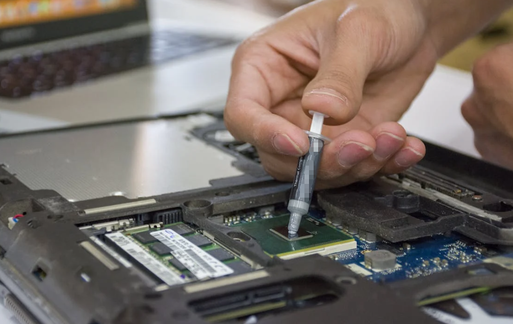
A copper shim is not automatically better than a thermal pad, even though copper has much higher bulk thermal conductivity. Copper is rigid. A thermal pad is compliant. That simple mechanical difference changes how each material contacts the heat source, handles gap variation, loads fragile components and behaves during assembly.
In a flat, tightly controlled interface, a correctly sized copper spacer with very thin interface material on both sides can work well. In an assembly with uneven component heights, uncertain tolerances, vibration or an electrical isolation requirement, a compressible pad is usually the safer choice.
So the real question is not, “Which material has the bigger W/mK number?” It is, “Which complete interface creates the lowest reliable resistance without damaging the assembly?” This guide works through that decision for GPUs, VRAM, laptops, power modules, telecom hardware and industrial electronics.
Copper Shim vs Thermal Pad: Quick Comparison
A copper shim favors high conductivity and dimensional stability, while a thermal pad favors conformity, electrical isolation and tolerance absorption. Copper can move heat efficiently through its body, but poor contact on either face can erase that advantage. A pad has lower conductivity, yet it can create more complete contact across rough, tilted or mixed-height surfaces.
| Decision Factor | Copper Shim | Thermal Pad |
| Bulk conductivity | Very high for suitable copper grades | Lower and formulation-dependent |
| Conformability | Rigid and unable to fill microscopic roughness alone | Compressible and able to follow surface variation |
| Gap tolerance | Needs tightly controlled thickness and geometry | Handles a wider working-gap range |
| Additional TIM | Usually needs a thin interface layer on both faces | Normally serves as the interface layer itself |
| Electrical behavior | Electrically conductive unless separately isolated | Electrically insulating grades are widely available |
| Mechanical load | Transfers displacement and force directly | Cushions variation, depending on hardness and compression |
| Production fit | Requires controlled placement and retention | Available as die-cut parts with liners and pull tabs |
| Typical best fit | Precise, stable and flat interfaces | Variable gaps, uneven arrays and fragile components |
This is a screening table, not a final specification. The answer can change when the actual gap, clamp load, surface finish or voltage requirement changes. A 0.2 mm error that looks tiny on a drawing may be enough to lift a heat sink away from a GPU die or overload a memory package.
What Is a Copper Shim, and What Is a Thermal Pad?
A copper shim is a rigid metal spacer used to bridge a controlled distance in a heat path. A thermal pad is a soft, filled polymer sheet designed to deform and make contact over a range of gaps. Both can conduct heat, but they solve different mechanical problems. Treating them as drop-in substitutes is where many cooling jobs go wrong.
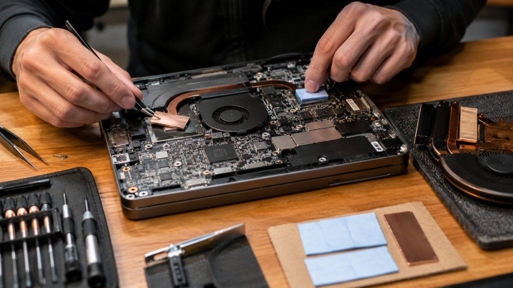
Copper shims are rigid heat-conducting spacers
A thermal copper shim is usually a thin, flat piece of copper cut or stamped to size. Common choices include C110 copper, oxygen-free copper and nickel-plated copper. The metal may be supplied in precise thicknesses, but its performance also depends on flatness, burr height, surface roughness, oxidation and the way it is held in place.
Copper bridges the visible gap. It does not naturally fill microscopic valleys on a chip, heat spreader or heat sink. Even two parts that look mirror-flat have high points and low points. When a bare shim touches those high points, much of the apparent area can still contain air. That is why copper shim assemblies commonly use a very thin layer of thermal grease, phase-change material or another conformable TIM on both faces.
Those extra layers are part of the design. Their thickness and coverage cannot be ignored. The shim also needs clean edges, enough clearance from nearby components and positive retention so it cannot slide into exposed circuitry.
Thermal pads are compliant gap-filling interfaces
A thermal pad generally combines a silicone or silicone-free polymer matrix with thermally conductive ceramic filler such as alumina or boron nitride. The balance of polymer, filler and reinforcement controls conductivity, hardness, tack, dielectric behavior, compression set and long-term stability.
When compressed, a pad follows surface texture and component-height variation. It can contact several VRAM packages or MOSFETs even when they do not sit in exactly the same plane. The pad may also provide electrical insulation and vibration cushioning. These are useful jobs that a plain copper plate cannot perform.
Pads are supplied in sheets, rolls and custom converted parts. Thickness, Shore 00 or Shore OO hardness, compression-deflection behavior, liner design and placement accuracy all matter. Haktak’s thermal pad product family covers standard and application-specific gap-filling formats for electronics assemblies.
Why Copper’s Higher W/mK Does Not Automatically Mean Lower Interface Resistance

Thermal conductivity describes how readily heat moves through a material. It does not describe the complete joint. A working interface also includes contact resistance at both surfaces. Copper can be a very fast path through the middle, but if it touches poorly at either end, the complete stack may perform worse than a softer pad with fuller contact.
A simplified model is: R_total = R_contact 1 + t/(kA) + R_contact 2
Here, t is material thickness, k is thermal conductivity and A is effective area. The middle term is the material’s bulk resistance. The two contact terms represent imperfect contact at its faces.
Think of copper as a wide, fast highway. If there is a traffic jam at both entrance ramps, widening the road in the middle does not fix the whole trip. Thermal grease can help open those ramps by filling microscopic voids, but it adds material and must remain thin. Too much paste becomes another resistive layer. Too little may leave dry spots.
Contact resistance changes with surface roughness, flatness, pressure, wetting and actual contact area. A rigid shim on a slightly tilted surface may touch strongly at one edge and barely touch elsewhere. A soft pad can often follow that tilt, although excessive pad thickness or hardness can create its own pressure problem.
This distinction is why engineers compare thermal conductivity with thermal impedance rather than selecting from W/mK alone. The official ASTM D5470-17(2024) method measures thermal transmission properties under stated test conditions. Pressure, thickness, specimen preparation and contact behavior need to be considered when comparing results.
A short illustrative calculation, not a performance promise
Imagine a 20 mm by 20 mm interface. Compare a 1 mm copper spacer at a hypothetical 390 W/mK with a 1 mm pad at a hypothetical 6 W/mK. If we calculate only bulk resistance, the copper term is far lower:
- Copper bulk term: 0.001 / (390 x 0.0004), about 0.0064 K/W
- Pad bulk term: 0.001 / (6 x 0.0004), about 0.417 K/W
That looks decisive. It is not the whole result. The copper assembly still has two copper-to-TIM contacts and two thin interface layers. If the shim tilts, the paste is thick, or clamp pressure is uneven, those contact terms may dominate. The pad may show higher bulk resistance but better real contact.
The numbers above are only a physics illustration. They are not a promised temperature reduction or a product comparison. A useful test has to reproduce the actual thickness, pressure, area, orientation and aging profile.
The Mechanical Difference Is Often More Important Than the Thermal Difference
Copper and thermal pads respond very differently to dimensional error. A copper shim transfers its thickness and load almost directly into the assembly. A pad deforms and absorbs some variation. That makes gap tolerance, package strength, PCB bending and clamp pressure central selection criteria, not side notes after a conductivity decision.
Gap tolerance and parallelism
The thickness printed on a removed pad is not necessarily the working gap. Pads are normally installed under compression. A nominal 1.5 mm pad may have operated at a smaller compressed thickness, and the compression may not have been equal across the part.
Measure the minimum, nominal and maximum assembled gap across several units. Include component-height tolerance, solder thickness, housing flatness, heat-sink tilt, fastener position and thermal expansion. If the gap changes across the interface, one uniform metal shim can become a hard pivot point.
Pressure, package stress and PCB bending
A rigid shim does not forgive much extra stack height. If it is too thick, it can load an exposed die, VRAM package, BGA solder joints or a thin PCB. It may also prevent the cooler from contacting a neighboring component. This is why a GPU core sometimes becomes hotter after someone “improves” the memory interface.
Pads absorb variation, but they are not harmless pillows. A hard pad or excessive compression can still create high force. The effect of compression on thermal pad performance must be balanced against the safe load of packages, solder joints and the board.
NASA’s overview of small-spacecraft thermal control makes a useful general point: interface conductance depends on contact pressure, and bolted joints do not necessarily create uniform pressure. The same principle applies to a heat sink fixed by screws or spring clips. Torque alone does not prove that every component has good contact.
Electrical isolation and placement safety
Copper conducts electricity. That may be acceptable on an isolated heat spreader, but it becomes a serious hazard near passives, solder joints, test points and exposed traces. The design must consider creepage, clearance and the possibility of a loose shim moving after shock or service.
An insulating coating or film can reduce electrical risk, but it becomes another layer in the thermal stack. Its dielectric strength, thickness, adhesion and puncture resistance need validation. Where heat transfer and insulation must come from one placed part, electrically insulating thermal pads are often easier to control.
Where a Copper Shim Can Make Sense

A copper shim is most defensible when the gap is stable, both surfaces are flat and parallel, clamp load is controlled, and electrical conduction is either acceptable or deliberately isolated. In that environment, the shim behaves as an engineered spacer. It is less convincing when it is used to guess at an unknown gap during a repair.
Controlled heat-spreader interfaces
A machined assembly with tight dimensional control can make good use of a copper spacer. The design should specify copper grade, thickness tolerance, flatness, edge condition and retention. Very thin interface layers can then address microscopic roughness on both sides.
Nickel plating may be considered where oxidation, repeated handling or surface compatibility matters. Plating changes the surface and should be included in thermal and adhesion testing. It is not simply cosmetic.
Repairing a known mechanical gap
A laptop, mini PC or embedded device may have a real stand-off problem between a package and its cooler. If measurements show a stable gap, a copper shim can correct that geometry. This is first a mechanical repair, then a thermal change.
Internet reports of large temperature drops can be useful clues, but they are not transferable specifications. The original pad may have been damaged, the cooler may have been poorly seated, or the reported sensor may not represent the hottest location. Copying another user’s shim thickness without measuring your own unit is a gamble.
Hybrid metal-spreader designs
A designed copper plate with thin compliant TIM can reduce the amount of low-conductivity material across a larger, well-controlled gap. This can make sense in power electronics and heat-spreader structures.
What usually does not make sense is an improvised stack of thick pad, loose shim and another thick pad. Every extra layer adds an interface and another tolerance. If the gap is large and irregular, a conformable material or a redesigned spreader is normally easier to validate.
Where a Thermal Pad Is Usually the Better Choice
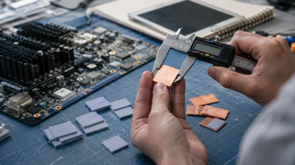
A thermal pad is normally safer when an assembly needs compliance, electrical insulation, vibration tolerance or repeatable production placement. Pads are especially useful across multiple components because they accommodate modest height differences without turning the highest component into a rigid stop. The correct pad still needs controlled thickness, hardness and compression.
GPUs, VRAM and mixed-height component arrays
Memory packages around a GPU rarely form a perfect plane. Board flex, package tolerance, solder and cooler flatness all contribute. A pad can distribute contact over the array. A single rigid plate may load one high package and leave a lower one with weak contact.
The pad must also avoid lifting the cooler away from the GPU die. That means core temperature, memory temperature and mechanical imprint should be checked together. One improved sensor does not prove that the whole assembly is healthier.
Power electronics, telecom and industrial enclosures
MOSFETs, IGBT modules, baseband processors, RF devices, LED boards and sealed controllers often transfer heat to a metal housing. These products see vibration, thermal cycling and enclosure movement. A pad can maintain contact as the stack expands and contracts.
Serviceability matters too. A pre-cut pad can remain attached to one surface or be replaced as a controlled part. Grease around a loose metal shim may be harder to inspect and reproduce on a production line.
Electrically sensitive interfaces
Insulating thermal pads can combine a heat path with dielectric separation. The specification should include thickness, breakdown behavior, defects, compression and the intended voltage environment. A catalog dielectric number is not permission to ignore creepage and clearance in the assembly.
Repeatable production and custom shapes
Pads can be supplied with holes, slots, tabs, selective tack and liners. These details reduce placement errors and support manual or automated assembly. Thermal pad die cutting and custom shapes can also keep material away from connectors, fasteners and keep-out zones without requiring operators to trim parts at the line.
How to Select Copper Shim or Thermal Pad Thickness Safely
Choose thickness from the assembled gap and allowable pressure, not from the uncompressed part that came out of the device. For a pad, define a target compressed thickness across the full tolerance range. For copper, account for both thin interface layers and verify that the rigid stack cannot overload components or disturb neighboring contacts.
Step 1: Measure the assembled gap range
Start with drawings if they exist, then check real assemblies. Gauge methods, pressure-sensitive film, controlled clay or putty checks, coordinate measurements and careful teardown evidence can all help. The method must not distort the gap it is trying to measure.
Record minimum, nominal and maximum values across several samples. Map the gap at more than one point if the surfaces may tilt. One measurement in the center can hide a large edge difference.
Step 2: Define the safe pressure window
Identify the weakest part of the stack. That might be an exposed die, a memory package, a BGA joint, a connector, a thin PCB or a plastic housing boss. Include fastener torque, spring-clip force and tolerance accumulation.
For pads, use compression-deflection data rather than hardness alone. Hardness is useful, but it does not directly state the force generated at a chosen compression.
Step 3: Size a thermal pad by compressed thickness
Nominal thickness is the supplied gauge. Working thickness is what remains after assembly. The thermal pad thickness selection guide explains why the selected pad must cover the largest gap without becoming too highly compressed at the smallest gap.
There is no universal compression percentage for every pad. Formulations behave differently. Use the supplier’s compression-deflection curve and establish an allowable thermal pad compression ratio for the actual assembly.
Step 4: Size a copper shim as part of a complete stack
Do not copy the nominal thickness of a removed pad. First estimate the operating gap. Then include the planned thermal grease or film on each face, shim thickness tolerance, plating and surface variation.
Avoid stacking several loose shims to reach a target. They can slip, trap contamination and create additional contacts. If multiple metal layers are necessary, they need a deliberate retention and interface design.
Step 5: Verify contact everywhere
Inspect the contact pattern before trusting temperature data. Look for a complete, appropriately thin paste imprint on both shim faces or an even pad impression across the interface. Check that adjacent components still contact their intended cooling surfaces.
Measure temperatures under a realistic power profile. A no-load desktop reading is not enough for a GPU, inverter or radio that spends time at high power.
Installation and Validation: A Practical Workflow
A useful comparison controls cleaning, placement, clamp load and test conditions. Otherwise, assembly variation can look like a material difference. Inspect contact before thermal testing, then repeat the relevant checks after cycling or vibration. The goal is not one impressive initial temperature. It is a stable interface that can be built again.
- Clean and inspect both surfaces. Remove old compound without scratching the heat spreader or cooler.
- Confirm shim or pad dimensions, orientation, edge clearance and liner removal.
- Apply the specified amount of grease to each shim face, or handle the pad without contaminating it.
- Assemble with a controlled torque sequence, spring load or fixture pressure.
- Inspect the contact pattern on an engineering sample before relying on temperature readings.
- Run the actual power profile and compare all relevant components, not only one sensor.
- Recheck thermal, mechanical and electrical behavior after the required aging profile.
| Validation Item | Useful Measurement | Acceptance Basis | Typical Failure Signal |
| Interface contact | Paste imprint, pressure film or pad impression | Continuous contact in required area | Dry corners, edge loading or untouched regions |
| Mechanical load | Clamp force, torque, PCB strain or package limit | Within drawing and component limits | Bowing, cracked package or shifted connector |
| Thermal result | Case, junction, memory and housing temperatures | Meets limits under real power and ambient | One sensor improves while another worsens |
| Electrical safety | Clearance, insulation resistance or dielectric test | Meets product voltage requirement | Intermittent short, puncture or conductive debris |
| Reliability | Post-cycle thermal retest and teardown | Stable contact and acceptable drift | Shim movement, pump-out, compression set or cracking |
For an application-specific program, Haktak’s material selection and testing support can combine thermal screening with mechanical, electrical and environmental checks.
Common Failure Modes and What They Usually Mean
Most failures point back to contact, stack height or mechanical load. A poor temperature after reassembly does not automatically mean the selected material has low conductivity. Start by checking imprint, cooler parallelism and the complete stack. Then inspect electrical clearance and signs of movement or aging.
| Observed Problem | Likely Copper-Shim Cause | Likely Thermal-Pad Cause | What to Check First |
| Temperature rises after reassembly | Poor paste coverage or wrong shim thickness | Wrong thickness, low compression or liner left on | Contact imprint and full stack height |
| GPU core becomes hotter after VRAM work | Shim lifts cooler away from the die | Pads are too thick or too hard | Core contact and cooler parallelism |
| One component is hotter than its neighbors | Height variation or tilted shim | Uneven compression or cut-part placement | Gap map and pressure distribution |
| Intermittent electrical fault | Copper edge touches circuitry or debris moves | Insulating layer is damaged or punctured | Clearance and dielectric condition |
| Performance degrades after cycling | Paste pump-out, shim movement or oxidation | Compression set, cracking or bleed | Post-aging teardown and thermal retest |
The broader guide to why thermal pads fail covers thickness error, poor storage, contamination and long-term mechanical change. If the proposed fix is simply adding layers, read whether thermal pads can be stacked first. Additional interfaces make alignment and compression harder to predict.
Standards and Data That Make Comparisons More Trustworthy
Useful comparisons state thickness, pressure, contact area, test method and aging condition. Thermal conductivity alone is not enough. Ask a pad supplier for impedance and compression data, and ask a shim supplier for alloy, tolerance, flatness and edge quality. Then validate the finished joint because material data does not reproduce every real enclosure or cooler.
ASTM D5470 is widely used to characterize thermal transmission properties of interface materials. It is useful because it recognizes that pressure and contact matter. It does not guarantee the same performance in a GPU cooler, power module or outdoor controller with different surfaces and loads.
For a thermal pad, request:
- Thickness and tolerance
- Thermal conductivity test method
- Thermal impedance at stated pressure and thickness
- Hardness method and value
- Compression-deflection curve
- Dielectric strength or breakdown data where needed
- Compression set, thermal aging and environmental conditions
For a copper shim, request:
- Copper alloy and conductivity basis
- Thickness and tolerance
- Flatness and surface roughness
- Burr and edge-control specification
- Plating type and thickness, if used
- Cleanliness, packaging and oxidation controls
The Copper Development Association’s official C11000 copper alloy data provides useful context for the metal’s conductivity and physical behavior. Those properties explain why copper is attractive, but the final thermal joint still has to be tested as an assembly.
Copper Shim vs Thermal Pad Selection Checklist
Choose a thermal pad when the gap varies, the parts are fragile or electrical isolation is required. Evaluate a copper shim stack when dimensions are precise, surfaces are flat, load is controlled and thin interface layers can be applied consistently. If neither option fits the geometry, reconsider the interface instead of forcing a material into the wrong job.
Work through these questions in order:
- Is electrical insulation required at the interface?
- Does the gap vary between locations, units or operating temperatures?
- Can the assembly tolerate rigid load transfer?
- Are both surfaces flat and parallel enough for a shim?
- Can thin interface layers be applied with repeatable coverage?
- Is the shim positively retained against movement?
- Does the design survive thermal cycling, shock and vibration?
- Can placement and contact be inspected in production?
Three practical outcomes follow:
- Choose a thermal pad for variable gaps, low-pressure interfaces, mixed-height arrays and electrical isolation. If pressure is a concern, compare soft and hard thermal pads using compression-deflection behavior, not feel alone.
- Evaluate a copper shim stack for precise, stable interfaces where load and retention are engineered.
- Consider another gap-filling approach when the gap is large, irregular or changes across components. The comparison of thermal putty and thermal pads for uneven gaps explains one alternative.
What to Send Haktak for a Material Recommendation
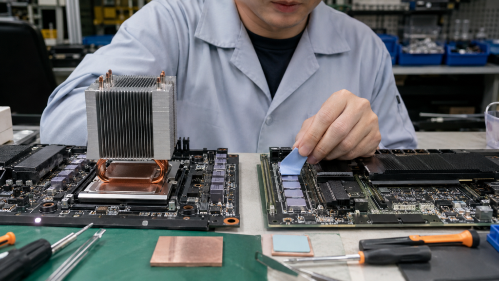
A useful recommendation starts with the mechanical drawing and operating conditions, not just a target conductivity. Share the gap range, heat load, cooling surface, pressure limit, voltage requirement and reliability profile. With those inputs, Haktak can screen the wider TIM family and recommend a pad, putty, grease or custom format for validation.
Please include:
- Drawing, interface area and keep-out zones
- Minimum, nominal and maximum assembled gap
- Heat source, power and temperature target
- Heat sink, cold plate or housing material and flatness
- Screw, clip or fixture method and pressure limit
- Voltage, dielectric and grounding requirements
- Operating temperature, humidity, vibration and service-life target
- Prototype quantity, production volume and preferred packaging
Review the broader range of thermal interface materials or request a thermal interface recommendation with your drawing and operating conditions.
Frequently Asked Questions
These questions cover the practical issues buyers, engineers and repair technicians raise most often. The short version is simple: copper is rigid and conductive; pads are compliant and can be insulating. Thickness, contact pressure and the full assembly determine whether either option works safely.
1. Is a copper shim better than a thermal pad?
Only in the right mechanical design. Copper has much higher bulk conductivity, but a shim needs controlled thickness, flat surfaces, suitable pressure and thin interface material on both faces. A thermal pad is usually more forgiving where gaps vary, components are fragile or electrical isolation is required. Compare total interface resistance and reliability, not conductivity alone.
2. Does a copper shim need thermal paste on both sides?
Usually, yes. The paste fills microscopic surface roughness between the heat source and shim, then between the shim and cooler. Use a thin, controlled layer. Paste should remove air, not become a thick gap filler. The exact interface material and application amount should be validated for the temperature, pressure and service life.
3. How do I choose the correct copper shim thickness?
Measure the assembled gap, including its minimum and maximum tolerance. Subtract the intended thin interface layers and check that the resulting stack does not create excessive force. Do not simply copy the nominal thickness printed on a removed thermal pad because that pad probably operated in a compressed state.
4. Can I replace GPU or VRAM thermal pads with copper shims?
It is possible in a carefully measured design, but it carries real risk. A wrong shim can lift the cooler from the GPU die, bend the PCB, load memory packages or cause an electrical short. VRAM heights can also vary. Check the full cooler contact pattern and all component temperatures before calling the modification successful.
5. Can a copper shim crack a GPU die or bend a PCB?
Yes. Copper transfers load directly because it does not compress like a pad. An oversized shim or uneven cooler can create a hard point over a package. Exposed dies are especially sensitive. Define the gap and pressure window first, then inspect board strain, cooler parallelism and contact during validation.
6. Are copper shims electrically conductive?
Yes. A copper shim can short exposed contacts, nearby passives or PCB features if it is misplaced or moves. Maintain edge clearance and use positive retention. If insulation is added, include that film or coating in thermal and dielectric testing because it changes both resistance and stack thickness.
7. Can I put a thermal pad on both sides of a copper shim?
Only as part of a designed large-gap stack. Thin compliant layers can help a metal spreader contact imperfect surfaces, but two thick pads plus a loose shim create extra interfaces and uncertain compression. A single suitable pad, thermal putty or redesigned heat spreader may be more repeatable.
8. Can thermal pads be stacked instead of using a thicker pad?
Stacking is generally less predictable than using one correctly sized pad. The layer boundary adds contact resistance, and the pads can shift or compress unevenly. For a prototype emergency it may reveal whether more gap filling is needed, but production should use a validated single thickness or another designed interface.
9. Which lasts longer, a copper shim or a thermal pad?
The copper body itself can remain stable for a long time, but the complete shim assembly still includes paste, plating, retention and nearby materials that can age. A pad’s life depends on formulation, compression set, temperature and cycling. Neither option has a universal life advantage without a defined environment and test profile.
10. How should I test a copper shim or thermal pad before production?
Check contact and pressure first, then measure all relevant component temperatures under realistic power and ambient conditions. Add electrical testing where insulation matters. Repeat thermal measurements after cycling, vibration or aging, then perform a teardown. Look for movement, pump-out, cracking, bleed, permanent compression and changes in contact imprint.