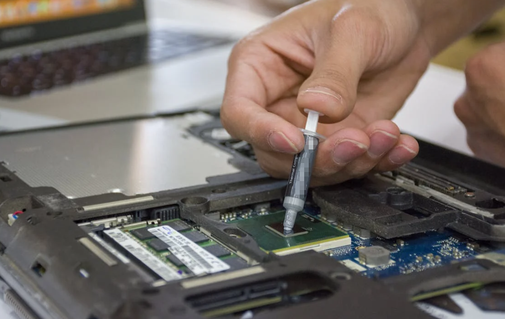
A phase change material and a conventional thermal pad can look surprisingly similar on a workbench. Both may arrive as clean, die-cut sheets with release liners. Once installed, though, they solve different problems. A PCM is meant to soften and wet a thin, clamped interface. A traditional gap pad is meant to compress into a larger or less predictable space.
That difference is more useful than asking which material has the higher conductivity number. A great PCM cannot bridge a 2 mm component-height mismatch. A soft gap pad can fill that space, but it may add too much thickness to a tightly clamped processor interface. The right answer starts with the mechanical stack.
PCM Thermal Pad vs Traditional Thermal Pad: The Core Difference
A PCM thermal pad is usually the better starting point for a thin, flat interface that stays under pressure and reaches the material’s activation range. A traditional elastomeric thermal pad is generally better for larger gaps, uneven component heights and assemblies that need compliance or cushioning. Neither family is automatically superior, and electrical insulation must be confirmed by grade.

What counts as a PCM thermal pad?
A PCM thermal pad, also called a phase change thermal interface material, is handleable as a solid at room temperature. When the interface warms past its designed transition range, the matrix softens and wets microscopic surface features. It does not need to become a loose, freely running liquid to improve contact.
That wetting action can reduce contact resistance and create a thin final bond line. It works best when the mating surfaces are already close together and the mounting system maintains pressure. For a deeper look at the chemistry and transition behavior, see how PCM thermal pads soften and work at the interface.
What counts as a traditional thermal pad?
In this comparison, a traditional thermal pad means a compressible silicone or non-silicone elastomeric gap pad filled with thermally conductive particles. It stays as a compliant solid during service. Instead of flowing into a thin joint, it deforms under pressure to touch surfaces separated by a measurable gap.
These pads are useful around mixed component heights, PCB warp, enclosure tolerances and delicate packages. They are not the same as graphite heat-spreading sheets, mica insulators or ceramic washers. Haktak’s thermal pad category covers the broader range of compliant gap-filling formats.
| Decision factor | PCM thermal pad | Traditional thermal gap pad |
| Primary job | Wet a thin, clamped interface after activation | Fill a larger or variable gap through compression |
| Installed thickness | Usually thin and reduced after phase change | Selected around the working gap and compression target |
| Surface geometry | Best with flat, closely matched surfaces | Better for uneven heights and wider tolerances |
| Pressure | Needs maintained contact and adequate clamping | Needs controlled compression without excessive component stress |
| Cushioning | Limited | Often useful for shock, vibration and fragile components |
| Electrical insulation | Product-specific | Commonly available, but still product-specific |
| Rework | Depends on material and service procedure | Often straightforward, though reuse is not automatically approved |
| Typical locations | Processor lids, power-module baseplates and thin heat-spreader joints | VRAM, VRM, multi-height boards, housings and battery electronics |
Start With Interface Geometry, Not Conductivity
The shape of the space between the heat source and cooling surface should be checked before comparing datasheet conductivity. A thin, flat joint and a board with 1.5 mm of component-height variation are different engineering jobs. If the material cannot maintain contact across the real tolerance range, an impressive W/mK value will not rescue the design.
Thin, flat and tightly clamped interfaces
PCM becomes attractive when two surfaces are already close, reasonably flat and continuously clamped. Think of a lidded processor against a cold plate, or a power-module baseplate mounted to a machined heat sink. The material only needs to fill surface roughness and small flatness errors. It does not need to behave like a structural spacer.
The mounting system matters. Screws, clips or springs must keep the joint closed after thermal expansion, vibration and aging. If pressure disappears when the assembly cycles, softened PCM cannot jump across a newly opened gap.
Larger gaps and mixed component heights
A traditional gap pad is the more natural choice when the interface includes board warp, enclosure variation or components of different heights. Its starting thickness is selected so the shortest path still makes contact while the tallest component is not overloaded.
This is why “use a 1 mm pad” is not enough information. Engineers need the minimum, nominal and maximum assembled gap, not only the CAD nominal. The practical steps in selecting thermal pad thickness for electronics explain how tolerance affects that decision.
A simple first-pass decision
- Measure the minimum, nominal and maximum working gap after assembly.
- Confirm whether pressure is maintained over the complete interface area.
- Check whether the interface reaches the PCM activation range in normal use or production.
- Define package-stress and PCB-deflection limits.
- Confirm dielectric, flame and restricted-chemistry requirements.
- Compare material families only after those boundaries are known.
How the Materials Move Heat in Different Ways
PCM and elastomeric pads both use conductive fillers, but their matrices behave differently. PCM improves contact by softening and wetting a thin joint at temperature. A conventional gap pad improves contact by elastic deformation under compression. One is closer to a heat-activated interface film; the other works more like a soft, conductive spacer.
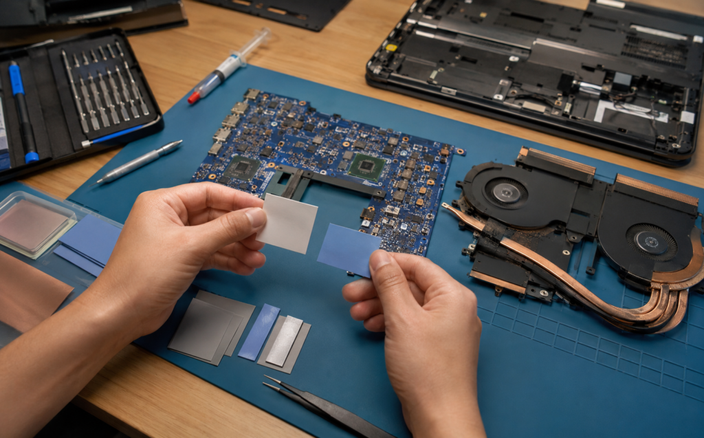
PCM structure and activation
A typical electronic PCM combines a polymeric or phase-change matrix with ceramic or other thermally conductive fillers. The exact chemistry, transition range and flow control vary by product. Some grades include a carrier, reinforcement or pressure-sensitive layer to improve handling.
The first meaningful thermal excursion can be important. For example, an Infineon application note for a pre-applied PCM describes a product-specific activation process and qualification tests. Its values should not be copied to unrelated materials, but the lesson is useful: activation conditions belong in the assembly plan, not in a footnote.
Elastomeric gap-pad structure
A conventional pad normally uses a silicone or alternative elastomer loaded with thermally conductive ceramic particles. Filler level affects conductivity, but it can also influence hardness, tear strength and conformability. Reinforcement may improve handling while changing how easily the pad compresses.
Surface tack, release liners and optional adhesive also matter on the production floor. A material that looks excellent in a coupon test can be awkward if operators cannot remove the liner cleanly or place a large die-cut shape without stretching it.
Here is a rough analogy. PCM is like a fitted gasket that settles into tiny surface marks when warmed. A gap pad is more like a soft shoe insole that takes up space and spreads load. The analogy is not perfect, but it points to the key difference: wetting a joint is not the same job as bridging a gap.
Thermal Performance Depends on Bond Line, Wetting and Pressure
Installed thermal resistance depends on more than bulk conductivity. Material thickness, contact resistance, pressure, surface roughness and interface area all shape the result. A PCM with a modest W/mK value may beat a thicker pad in a controlled joint. That same PCM may fail badly if the assembly leaves an open gap that it cannot bridge.

Why W/mK alone can mislead
Thermal conductivity describes a bulk material property under a stated test condition. It does not directly tell you the temperature rise across a finished interface. A complete comparison should include thermal impedance or resistance at the intended thickness and pressure.
This distinction is easy to miss during sourcing because W/mK is a clean number that fits neatly in a spreadsheet. The guide to thermal conductivity versus thermal impedance in TIM selection shows why the larger number is not always the cooler result.
Bond-line thickness can dominate the result
All else equal, heat has an easier path through a thinner layer. PCM is attractive partly because it can form a very thin installed bond line after activation. A conventional pad needs enough thickness to cover the actual gap and tolerance stack, so its heat path may be longer.
But “thinner is better” only applies after contact has been secured. A layer that is too thin to touch both surfaces is simply an air gap. For the underlying relationship, review how bond-line thickness changes thermal performance.
Contact resistance is the quiet part of the problem
Machined metal may look smooth, yet the surfaces touch at microscopic high points. Air remains in the valleys, and air is a poor heat-transfer medium. PCM can wet those fine features after softening. A compliant pad presses into them while also taking up larger geometric variation.
That is why the best comparison is an assembly temperature or interface-resistance test at controlled power, pressure and cooling conditions. A catalog number cannot see your surface finish, screw pattern or warped PCB.
Gap Size, Compression and Mechanical Stress
Traditional pads need enough compression to make stable contact, but not so much that they bend the PCB or overload packages and solder joints. PCM also needs pressure, although it is not normally selected as a thick compression element. In both cases, the mounting design and material behavior must be evaluated together.
Compression is a design variable
For a soft pad, engineers should review compression-deflection data rather than choosing a percentage by habit. Two materials with the same thickness and hardness label can create different forces because their formulations, filler loading and test methods differ.
Too little compression can leave incomplete contact. Too much can bow the board, crack brittle components, damage solder joints or squeeze the material beyond its intended condition. Haktak’s guide to thermal pad compression ratio and assembly pressure covers this trade-off in more detail.
PCM still needs mechanical control
PCM does not remove the need for a sound clamp. The joint must close before activation and remain closed afterward. Excessive pressure may move softened material toward the edges, while poor pressure distribution can leave dry areas. Large unsupported spans can also distort a package or cold plate.
In short, PCM is not self-leveling construction filler. It is a thin-interface material.
Electrical Insulation and Compatibility Are Grade-Specific
Neither product family should be assumed electrically insulating simply because it is sold as a pad. Many conventional gap pads are designed for dielectric isolation, but the value still belongs to a particular grade and thickness. Some PCM constructions may permit very thin separation or near metal-to-metal contact after activation, which can be unacceptable in high-voltage hardware.

Check dielectric strength, volume resistivity and the test thickness used on the datasheet. Then compare those values with working voltage, creepage, clearance and fault conditions. If the TIM is part of an insulation system, test the finished stack after aging, not only a fresh material coupon.
Chemistry can matter too. Silicone pads are widely used because they are soft and stable, yet silicone-sensitive optical, coating, bonding or contact applications may require a non-silicone option. “Silicone-free” and “low siloxane” are also different claims. Ask the supplier what was measured and by which method.
Long-Term Reliability: Different Materials, Different Failure Modes
PCM and traditional pads can both provide long service when used in the right interface. Their risks are different. PCM qualification may focus on material movement, edge bleed, clamp retention and repeated thermal transition. Gap-pad qualification often focuses on compression set, hardening, tearing, vibration and loss of recovery.
What to watch with PCM
- Movement or edge migration during thermal cycling.
- Loss of contact if the clamp relaxes.
- Pump-out under cyclic expansion and contraction.
- Contamination of nearby surfaces.
- Orientation effects in vertical or inverted assemblies.
- Changes after repeated exposure above the transition range.
What to watch with a traditional pad
- Compression set and reduced recovery.
- Cracking, hardening or filler-related brittleness after aging.
- Pad walking or displacement under vibration.
- Loss of contact at the low end of the gap tolerance.
- Excessive force at the high end of the tolerance.
- Dielectric degradation in humid or contaminated conditions.
No single cycle count proves lifetime for every product. A telecom radio on a tower, a gaming GPU and an automotive inverter see different temperature swings, vibration and service conditions. Qualification should reproduce the dominant field stresses, then repeat thermal, mechanical, visual and electrical checks.
Assembly, Automation, Rework and Total Cost
Both families can be supplied as die-cut parts, rolls or pre-applied formats, but their process controls differ. PCM may need a defined activation step and post-activation inspection. Traditional pads require controlled thickness, liner removal and placement without stretching. Rework, storage, labor and yield often matter more than a small difference in piece price.

Handling and placement
For production, define which liner is removed first, how the part is located and how trapped folds or contamination are detected. Large soft pads may need tabs, reinforcement or array packaging. PCM may be supplied as a preform, coating or stencil-applied layer depending on the product.
Storage limits also need to follow the actual datasheet. Temperature, humidity, liner condition and shelf time can affect tack or handling. The same discipline used for thermal pad storage and shelf-life control should be part of incoming inspection and material rotation.
Rework and field service
A conventional pad can appear reusable because it remains in one piece. That does not mean reuse is approved. It may have taken a compression set, torn around components or collected dust. PCM can leave residue or require a fresh preform after the cooler is lifted.
Write the service rule before launch: inspect and reuse under defined conditions, or remove, clean and replace. A vague instruction such as “reuse if it looks fine” creates avoidable variation.
Where Each Material Usually Fits Best
PCM commonly starts ahead in thin processor, heat-spreader and controlled power-module interfaces. Traditional pads start ahead around VRAM, VRM, battery electronics and multi-height boards. One device can use both: PCM at a flat high-flux processor joint and soft pads around nearby components with larger gaps.
CPU and GPU interfaces
A lidded processor or controlled GPU interface may suit PCM when the cooler is flat, clamped and able to reach the activation range. The thin final layer can reduce contact resistance without the mess of grease. Bare-die hardware is more sensitive to pressure and geometry, so it should follow the device and cooler manufacturer’s requirements.
VRAM and VRM components
Memory and power-delivery components often sit at different heights from the main processor. Traditional pads bridge those offsets and tolerate board or cooler variation. Replacing a 1 or 2 mm memory pad with a thin PCM film can leave the memory untouched while changing the cooler load on the GPU. That is not an upgrade. It is a broken stack.
Power modules and inverters
PCM can work well between a flat module baseplate and heat sink when mounting pressure and activation are controlled. Nearby sensors, busbar regions or control boards may still need compliant pads. The best material can change within a few centimeters because the interface geometry changes.
LED, telecom, battery and industrial electronics
LED boards clamped to machined housings may use thin TIMs, while drivers and connectors often need gap filling. Outdoor radios add vibration, condensation and vertical orientation. Battery control electronics add large areas, tolerance and dielectric requirements. Choose by interface location, not by the product’s broad industry label.
| Assembly condition | Likely starting candidate | Why |
| Thin, flat, clamped processor interface | PCM | Thin final bond line and heat-activated wetting |
| Multi-height VRAM or VRM area | Traditional gap pad | Compliance across component-height variation |
| Power-module baseplate with controlled mounting | PCM, subject to qualification | Thin joint and repeatable clamp can favor low impedance |
| Warped PCB to metal enclosure | Traditional gap pad | Accommodates gap and flatness tolerance |
| Fragile package with a low stress limit | Very soft pad or another low-force gap filler | Compression force can be matched to package limits |
| High-voltage interface | Verified insulating grade only | Electrical performance is product-specific |
When You Should Not Swap One for the Other
A thick gap pad may be part of the mechanical stack, not just the thermal path. Replacing it with a thin PCM can leave an open gap or shift cooler pressure onto another component. Replacing PCM with a thick pad can increase thermal resistance and mounting force. Neither substitution should be made from dimensions on a web listing alone.
Before approving a swap, compare the assembled gap, pad compression, cooler height, fastener travel and contact pattern. Then measure temperature under the same power and cooling boundary. If any part of the cooler touches a second component, evaluate that load as well.
This is especially important in repair work. Online advice may recommend PCM for a GPU core while ignoring the memory-pad stack around it. The interface is a small mechanical system. Changing one layer can move everything else.
How to Qualify PCM and Traditional Thermal Pads

Compare candidates at the real installed thickness, pressure, heat load and environmental profile. Do not compare a PCM value measured in a thin clamped fixture with a gap-pad value measured at a different thickness and pressure, then declare a winner. Standardized coupon testing is useful, but the finished assembly still needs validation.
ASTM D5470 is a recognized reference for measuring thermal transmission properties of thermally conductive electrical insulation materials. The standard helps create comparable test discipline, but it does not reproduce every housing, screw pattern or power cycle. Haktak’s overview of common TIM testing standards for engineers explains where standardized methods fit.
A practical A/B test plan
- Freeze the mechanical stack, fastener pattern and mounting torque.
- Record actual gap, interface area and candidate thickness.
- Measure clamping pressure or a defensible proxy.
- Run a baseline at controlled power and cooling conditions.
- Apply the specified activation cycle to PCM candidates.
- Repeat thermal measurements after activation.
- Run relevant temperature, power, humidity and vibration aging.
- Recheck temperature, dielectric behavior, position and physical condition.
- Remove the cooler and inspect coverage, residue and serviceability.
Record the complete method. A result without pressure, thickness and boundary conditions is hard to reproduce and even harder to trust.
A Practical Selection Workflow for Buyers and Engineers
A supplier can recommend material faster when the request describes the assembly rather than asking for “the best thermal pad.” Provide the stack drawing, gap range, heat load, temperature limits, mounting method and electrical requirements. Add the production and reliability plan so the recommended grade can survive both the device and the factory.
Use this checklist:
- Heat source, power dissipation and allowable case or junction temperature.
- Cooling surface material, temperature and flatness.
- Minimum, nominal and maximum interface gap.
- Interface area, holes, keep-outs and nearby sensitive parts.
- Screw torque, clip load, pressure range and package-stress limit.
- Operating, peak and storage temperatures.
- Voltage, dielectric, flame and grounding requirements.
- Silicone restrictions, outgassing limits or coating compatibility.
- Placement method, activation process, inspection and rework plan.
- Thermal cycling, humidity, vibration and expected service life.
Haktak’s material selection and testing support can turn those inputs into a smaller candidate set and an application-level test plan. For thin, controlled joints, review the available phase change thermal interface material options after confirming the assembly can maintain contact and activation conditions.
Conclusion
PCM is mainly a thin-interface solution. A traditional thermal pad is mainly a compliant gap-management solution. PCM can deliver excellent contact and low thermal resistance in a flat, clamped joint. A gap pad can maintain contact where component heights, tolerances and vibration make a thin interface unrealistic.
So, which one should you use? Measure the assembled interface first. Then check pressure, activation temperature, electrical isolation, production handling and the likely aging mechanism. The material that fits those conditions is the better material, even if another option has a more exciting conductivity number.
For a drawing-based recommendation, send Haktak your gap range, thermal target and reliability requirements.
Frequently Asked Questions
Is a PCM thermal pad better than a traditional thermal pad?
Not in every assembly. PCM is often better for a thin, flat and continuously clamped interface. A traditional gap pad is usually better for larger gaps, mixed component heights and assemblies needing cushioning. Installed geometry and pressure decide which advantage matters.
Can a PCM thermal pad replace a silicone thermal pad?
Only when the silicone pad is not needed to bridge a significant gap or maintain the mechanical stack. Check the actual compressed thickness and cooler position first. A thin PCM cannot replace missing height.
Which material is better for CPU and GPU cooling?
PCM can suit a flat processor-to-cooler interface because it forms a thin bond line after activation. Traditional pads are more common around VRAM and VRM parts where height varies. Follow device and cooler requirements, especially on bare dies.
Can PCM replace thermal pads on VRAM or VRM components?
Usually not as a direct substitution. Memory and power components often need a relatively thick, compressible material to meet the cooler. Using thin PCM can leave those parts without contact and may alter pressure on the main processor.
Which material is better for large or uneven gaps?
A compliant traditional gap pad is normally the better starting point. Choose thickness and softness around the complete tolerance range, then verify that maximum compression does not overload the PCB or package.
Does a PCM thermal pad need pressure and an activation cycle?
It normally needs maintained pressure, and many products need to reach a defined temperature so the matrix softens and wets the surfaces. The exact temperature, duration and procedure are grade-specific, so use the supplier’s data.
Are PCM thermal pads electrically insulating?
Some are, while others should not be treated as an insulation barrier. Check dielectric strength, volume resistivity and final thickness for the exact grade. Validate the finished assembly when electrical isolation is safety-critical.
Which lasts longer, PCM or a traditional thermal pad?
There is no universal winner. PCM life depends on clamp retention, cycling and material movement. Gap-pad life depends on compression set, hardening, vibration and environmental exposure. Test the conditions that match the real product.
Can either thermal pad be reused after removing the heat sink?
Do not assume so. A conventional pad may be torn, contaminated or permanently compressed. PCM may have changed shape or left residue after activation. Follow the service specification; replacement is often the more repeatable choice.
Does a higher W/mK rating always mean better cooling?
No. Final cooling also depends on bond-line thickness, contact resistance, pressure and coverage. A lower-conductivity material can perform better if it creates a thinner, more complete interface under the actual assembly conditions.